 | –≠–ª–µ–∫—Ç—Ä–æ–Ω–Ω—ã–π –∫–æ–º–ø–æ–Ω–µ–Ω—Ç: PLL202-03 | –°–∫–∞—á–∞—Ç—å:  PDF PDF  ZIP ZIP |
PLL202-03
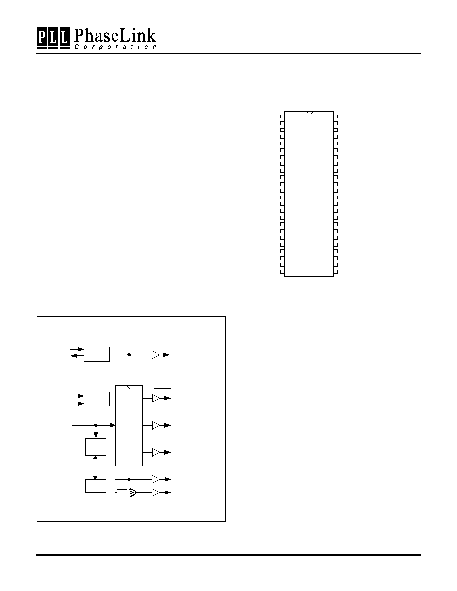
Motherboard Clock Generator for SIS540/630 with 133MHz FSB
47745 Fremont Blvd., Fremont, California 94538 TEL (510) 492-0990 FAX (510) 492-0991 Rev 02/15/00 Page 1
FEATURES
∑
Generates all clock frequencies for SIS540,
SIS630 Pentium
/
and K6 chip sets,
requiring multiple CPU clocks and high speed
SDRAM buffers.
∑
Support 3 CPU clocks, 7PCI and 14 high-speed
SDRAM buffers for 3-DIMM applications.
∑
One I2C selectable 24 or 48MHz clock output
(default 24 MHz).
∑
One 48 MHz USB clock output.
∑
Two14.318MHz reference clocks.
∑
Support 2-wire I2C serial bus interface with built-
in Vendor ID, Device ID and Revision ID.
∑
Single byte micro-step linear Frequency Progra-
mming via I2C with Glitch free smooth switching.
∑
Spread Spectrum
±
0.25% center or -0.5% down.
∑
50% duty cycle with low jitter.
∑
Available in 300 mil 48 pin SSOP.
BLOCK DIAGRAM
PIN CONFIGURATION
Note:
v
: Pull down
*
: Bi-directional latched at power-up
POWER GROUP
∑
VDD0: PLL CORE
∑
VDD1: REF(0:1), XIN, XOUT
∑
VDD2: PCI(0:6)
∑
VDD3: SDRAM(0:13)
∑
VDD4: 48MHz, 24_48MHz
∑
VDDL1: CPU(0:2)
KEY SPECIFICATIONS
∑
CPU Cycle to Cycle jitter: 250ps.
∑
PCI to PCI output skew: 500ps.
∑
CPU to SDRAM output skew: 500ps.
∑
CPU to CPU output skew: 250ps.
∑
SDRAM to SDRAM output skew: 250ps.
∑
CPU to PCI skew (CPU leads): 1 ~ 4 ns.
SDRAM13
SDRAM12
GND
SDRAM11
SDRAM10
VDD3
SDRAM9
SDRAM8
GND
SDRAM7
SDRAM6
SDATA
1
2
3
4
5
6
7
8
9
10
11
12
13
14
15
16
17
18
19
20
21
22
23
24
PLL202-03
REF1
VDDL1
CPU0
CPU1
GND
CPU2
VDD3
VDD3
SDRAM5
SDRAM4
VDD4
48MHz/FS0*
v
24_48MHz/CPU2.5_3.3*
v
SCLK
GND
VDD2
PCI6
GND
PCI2
PCI1/FS2*
v
PCI0/FS1*
v
VDD1
XOUT
XIN
GNDREF
REF0/FS3*
v
VDD0
48
47
46
45
44
43
42
41
40
39
38
37
36
35
34
33
32
31
30
29
28
27
26
25
PCI3
PCI4
PCI5
1
2
3
4
5
6
7
8
9
10
11
12
13
14
15
16
17
18
19
20
21
22
23
24
48
47
46
45
44
43
42
41
40
39
38
37
36
35
34
33
32
31
30
29
28
27
26
25
SDRAM3
SDRAM2
VDD3
SDRAM1
SDRAM0
GND
48Mhz
FS (0:3)*
PLL1
SST
Control
Logic
VDD4
24_48Mhz
PLL2
SDATA
SCLK
I2C
Logic
VDD1
REF(0:1)
XIN
XOUT
XTAL
OSC
VDDL2
CPU(0:2)
SDRAM(0:13)
VDD2
PCI(0:6)
VDD3
2
˜

PLL202-03
Motherboard Clock Generator for SIS540/630 with 133MHz FSB
47745 Fremont Blvd., Fremont, California 94538 TEL (510) 492-0990 FAX (510) 492-0991 Rev 02/15/00 Page 2
PIN DESCRIPTIONS
Name
Number
Type
Description
VDD0
1
P
Power supply for PLL Core.
VDD1
6
P
Power supply for REF0, REF1, and crystal oscillator.
VDD2
15
P
Power supply for PCI (0:6).
VDD3
19,30,36,42
P
Power supply for SDRAM (0:13).
VDD4
27
P
Power supply for 24_48MHz and 48MHz.
VDDL1
47
P
Power supply for CPU (0:2) 2.5V.
GND
3,10,16,22,
33,39,44
P
Ground.
XIN
4
I
14.318MHz crystal input to be connected to one end of the crystal.
XOUT
5
O
14.318MHz crystal output.
REF0/FS3*
PCI0/FS1*
PCI1/FS2*
48MHz/FS0*
2,7,8,26
B
At power up, these pins are input pins and will determine the CPU clock
frequency. After input sampling, these pins will generate output clocks.
They have internal pull down (low by default).
PCI (0:6)
7,8,9,11,12,
13,14
O
PCI clocks with frequencies defined by Frequency Table.
CPU (0:2)
46,45,43
O
CPU clocks with frequencies defined by Frequency Table.
SDRAM (0:13)
17,18,20,21,28,
29,31,32,34,35,
37,38,40,41
O
SDRAM clocks with frequencies defined by Frequency Table.
SDATA
23
B
SCLK
24
I
Serial data input for serial interface port.
48MHz
26
O
48MHz output for USB after input data latched during power-up.
24_48MHz/
CPU2.5_3.3*
25
B
Clock output for SUPER I/O after input data latched during power-up. It
can be programmed by setting I2C byte1.bit7 to select either 24Mhz
(default) or 48Mhz. CPU2.5_3.3 input will program internal CPU skew
circuits based on CPU voltage. If high, it selects 2.5V. If Low, it selects
3.3V (default).
REF0
2
O
Buffered reference clock output after input data latched during power-up.
REF1
48
O
Buffered reference clock output.

PLL202-03
Motherboard Clock Generator for SIS540/630 with 133MHz FSB
47745 Fremont Blvd., Fremont, California 94538 TEL (510) 492-0990 FAX (510) 492-0991 Rev 02/15/00 Page 3
FREQUENCY (MHz) SELECTION TABLE
I2C
Byte0
bit7
FS3
FS2
FS1
FS0
CPU
SDRAM
PCI
Spread
Spectrum
Modulation
0
0
0
0
66.6
100.0
33.3
0 to -0.5%
0
0
0
1
100.0
100.0
33.3
0 to -0.5%
0
0
1
0
150.0
100.0
37.6
±
0.25%
0
0
1
1
133.3
100.0
33.3
0 to -0.5%
0
1
0
0
66.8
133.6
33.4
±
0.25%
0
1
0
1
100.0
133.3
33.3
0 to -0.5%
0
1
1
0
100.0
150.0
37.6
±
0.25%
0
1
1
1
133.3
133.3
33.3
0 to -0.5%
1
0
0
0
66.8
66.8
33.4
±
0.25%
1
0
0
1
97.0
97.0
32.3
0 to -0.5%
1
0
1
0
68.0
113.3
28.3
±
0.25%
1
0
1
1
95.0
95.0
31.6
±
0.25%
1
1
0
0
95.0
126.7
31.6
±
0.25%
1
1
0
1
112.0
112.0
37.3
±
0.25%
1
1
1
0
166.0
111.0
27.6
±
0.25%
0
default
1
1
1
1
96.2
96.2
32.1
0 to -0.5%
0
0
0
0
66.8
100.2
33.4
±
0.25%
0
0
0
1
100.2
100.2
33.4
±
0.25%
0
0
1
0
97.0
97.0
32.3
±
0.25%
0
0
1
1
100.2
133.6
33.4
±
0.25%
0
1
0
0
75.0
100.0
37.5
±
0.25%
0
1
0
1
83.3
125.0
31.2
±
0.25%
0
1
1
0
105.0
140.0
35.0
±
0.25%
0
1
1
1
133.6
133.6
33.4
±
0.25%
1
0
0
0
110.2
147.0
36.7
±
0.25%
1
0
0
1
115.0
153.4
38.3
±
0.25%
1
0
1
0
120.0
120.0
30.0
±
0.25%
1
0
1
1
138.0
138.0
34.5
±
0.25%
1
1
0
0
140.0
140.0
35.0
±
0.25%
1
1
0
1
145.0
145.0
36.2
±
0.25%
1
1
1
0
147.6
147.6
36.9
±
0.25%
1
1
1
1
1
160.0
160.0
26.6
±
0.25%

PLL202-03
Motherboard Clock Generator for SIS540/630 with 133MHz FSB
47745 Fremont Blvd., Fremont, California 94538 TEL (510) 492-0990 FAX (510) 492-0991 Rev 02/15/00 Page 4
FREQUENCY (MHz) SELECTION TABLE BY TIMING GROUP
Group
Timing
(CPU:SDRAM)
I2C
Byte0
bit7
FS3
FS2
FS1
FS0
CPU
SDRAM
PCI
Spread
Spectrum
Modulation
0
1
0
0
0
66.8
66.8
33.4
±
0.25%
0
1
0
1
1
95.0
95.0
31.6
±
0.25%
0
1
1
1
1
96.2
96.2
32.1
0 to -0.5%
0
1
0
0
1
97.0
97.0
32.3
0 to -0.5%
1
0
0
1
0
97.0
97.0
32.3
±
0.25%
0
0
0
0
1
100.0
100.0
33.3
0 to -0.5%
1
0
0
0
1
100.2
100.2
33.4
±
0.25%
0
1
1
0
1
112.0
112.0
37.3
±
0.25%
1
1
0
1
0
120.0
120.0
30.0
±
0.25%
0
0
1
1
1
133.3
133.3
33.3
0 to -0.5%
1
0
1
1
1
133.6
133.6
33.4
±
0.25%
1
1
0
1
1
138.0
138.0
34.5
±
0.25%
1
1
1
0
0
140.0
140.0
35.0
±
0.25%
1
1
1
0
1
145.0
145.0
36.2
±
0.25%
1
1
1
1
0
147.6
147.6
36.9
±
0.25%
A
(2:2)
1
1
1
1
1
160.0
160.0
26.6
±
0.25%
0
0
0
1
0
150.0
100.0
37.6
±
0.25%
B
(2:3)
0
1
1
1
0
166.0
111.0
27.6
±
0.25%
0
0
0
0
0
66.6
100.0
33.3
0 to -0.5%
1
0
0
0
0
66.8
100.2
33.4
±
0.25%
1
0
1
0
1
83.3
125.0
31.2
±
0.25%
C
(3:2)
0
0
1
1
0
100.0
150.0
37.6
±
0.25%
D (3:4)
0
0
0
1
1
133.3
100.0
33.3
0 to -0.5%
E (4:2)
0
0
1
0
0
66.8
133.6
33.4
±
0.25%
1
0
1
0
0
75.0
100.0
37.5
±
0.25%
0
1
1
0
0
95.0
126.7
31.6
±
0.25%
0
0
1
0
1
100.0
133.3
33.3
0 to -0.5%
1
0
0
1
1
100.2
133.6
33.4
±
0.25%
1
0
1
1
0
105.0
140.0
35.0
±
0.25%
1
1
0
0
0
110.2
147.0
36.7
±
0.25%
F
(4:3)
1
1
0
0
1
115.0
153.4
38.3
±
0.25%
G (5:3)
0
1
0
1
0
68.0
113.3
28.3
±
0.25%

PLL202-03
Motherboard Clock Generator for SIS540/630 with 133MHz FSB
47745 Fremont Blvd., Fremont, California 94538 TEL (510) 492-0990 FAX (510) 492-0991 Rev 02/15/00 Page 5
I2C BUS CONFIGURATION SETTING
Address Assignment
A6 A5 A4 A3 A2 A1 A0 R/W
1 1 0 1 0 0 1 _
Slave
Receiver/Transmitter
Provides both slave write and readback functionality
Data Transfer Rate
Standard mode at 100kbits/s
Serial Bits Reading
The serial bits will be read or sent by the clock driver in the following order
Byte 0 ≠ Bits 7, 6, 5, 4, 3, 2, 1, 0
Byte 1 ≠ Bits 7, 6, 5, 4, 3, 2, 1, 0
-
Byte N ≠ Bits 7, 6, 5, 4, 3, 2, 1, 0
Data Protocol
This serial protocol is designed to allow both blocks write and read from the controller. The
bytes must be accessed in sequential order from lowest to highest byte. Each byte transferred
must be followed by 1 acknowledge bit. A byte transferred without acknowledged bit will
terminate the transfer. The write or read block both begins with the master sending a slave
address and a write condition (0xD2) or a read condition (0xD3).
Following the acknowledge of this address byte, in
Write Mode: the Command Byte and Byte
Count Byte must be sent by the master but ignored by the slave, in Read Mode: the Byte
Count Byte will be read by the master then all other Data Byte.
I2C CONTROL REGISTERS
1. BYTE 0: Functional and Frequency Select Clock Register (1=Enable, 0=Disable)
Bit
Pin#
Default
Description
Bit 7
-
0
FS4 ( see Frequency selection Table )
Bit 6
8
0
FS2 ( see Frequency selection Table )
Bit 5
7
1
FS1 ( see Frequency selection Table )
Bit 4
26
0
FS0 ( see Frequency selection Table )
Bit 3
-
0
Frequency selection control bit 1=Via I2C, 0=Via External jumper
Bit 2
2
0
FS3 ( see Frequency selection Table )
Bit 1
-
1
0=Normal 1=Spread Spectrum enable
Bit 0
-
0
0=Normal 1=Tristate Mode for all outputs