
PLL202-108
Programmable Clock Generator for ALI 1681 P4 Chip Sets
47745 Fremont Blvd., Fremont, California 94538 TEL (510) 492-0990 FAX (510) 492-0991 Rev 8/20/02 Page 1
48Mhz
24_48Mhz
PD#
XIN
XOUT
SDATA
SCLK
MULTSEL
XTAL
OSC
I2C
Logic
PLL1
SST
Control
Logic
REF(0:1)
AGP (0:1)
PCI (0:8)
PCIF
PLL2
˜ 2
Watch
Dog
WDRESET#
VDD
VDD
VDD
VDDCPU
CPUT (0:1)
CPUC (0:1)
PCISTP#
CPUSTP#
FS(0:3)
HTTSEL
HTTT (0:1)
HTTC (0:1)
VDDHTT
FEATURES
∑ Supports ALI 1681 Pentium 4 Chipsets.
∑ Programmable Spread Spectrum Modulation
from
±0.1% to ±1.5% with step size as small as
±0.012%.
∑ Selectable Spread Spectrum either center or
down.
∑ Selectable Spread Spectrum modulation profile.
∑ AccuSkew
TM,
Programmable Precision skew
tuning channel with maximum
±5% precision
over the variation of temperature, process and
voltage with step size as small as 80ps.
∑ AccuDrive
TM
Programmable Output Buffer drive
strength with up to +50% or ≠40%.
∑ Programmable VCO frequency with one variable
∑ Programmable Output Divider for CPU, HTT,
AGP and PCI.
∑ 2 differential CPUCLK and HTT CLK, 2 AGP, 9
PCI, 1 USB and 2 REF clock outputs.
∑ 1 programmable 24MHz or 48MHz for SIO.
∑ Support 2-wire I2C serial bus interface.
∑ Built-in programmable watchdog timer
∑ Available in 300 mil 48 pin SSOP.
BLOCK DIAGRAM
PIN CONFIGURATION
Note:
^:
Pull Up (120k
),
v:
Pull down (120k
), #: Active low,
*
: Bi-directional latched at power-up
POWER GROUP
∑ VDDREF (3.3V), VSSREF: REF, XIN, XOUT
∑ VDDPCI (3.3V), VSSPCI: PCI
∑ VDDAGP (3.3V), VSSAGP: AGP
∑ VDD48M (3.3V), VSS48M: 48MHz, 24_48MHz
∑ VDDCPU (3.3V), VSSCPU: CPUT/C[0:1]
∑ VDDHTT (3.3V), VSSHTT: HTTT/C[0:1]
∑ AVDD (3.3V), AVSS: PLL Analog
KEY SPECIFICATIONS
∑ CPU - CPU Output Skew < 150ps.
∑ AGP - AGP Output Skew < 150ps
∑ PCI - PCI Output Skew < 500ps
∑ CPU (early) to PCI Skew: 1.5 to 2.5 ns (typ 2ns).
∑ AGP (early) to PCI Skew: 1.5 to 2.5 ns (typ 2ns).
∑ CPU to HTT Skew < 150ps.
∑ CPU to AGP Skew < 150ps.
∑ CPU outputs cycle to cycle jitter < 150ps.
∑ PCI outputs cycle to cycle jitter < 250ps.
∑ AGP outputs cycle to cycle jitter < 250ps.
∑ 48MHz outputs cycle to cycle jitter < 350ps.
PLL202-108
1
2
3
4
5
6
7
8
9
10
11
12
13
14
15
16
17
18
19
20
21
22
23
24
40
39
38
37
36
35
34
33
32
31
30
29
28
27
26
25
41
42
44
43
45
46
47
48
PCI0
48MHZ/FS3*
V
PCI1
VSSPCI
PCI2
PCI4
XIN
REF0/FS2*
V
PCI6/MULTSEL*
V
PCI5/HTTSEL*^
PCI3
VDDPCI
24_48MHz/MODE*^
VDD48M
VDDREF
PCI8//PCISTOP#^
PCI7/FS1*
V
VSSPCI
VDDPCI
PCIF/SEL24_48#*^
VSS48M
REF1/FS0*
V
VSSCPU
CPUT1
WDRESET#
IREF
AVSS
AVDD
CPUCTP#^/Vtt_pwrgd
SDATA
VDDHTT
VSSHTT
VSSAGP
AGP1
SCLK
CPUT0
CPUC0
CPUC1
PD#^
HTTT0
HTTC0
HTTT1
HTTC1
VDDAGP
AGP0
VDDCPU
XOUT
VSSREF
PLL202-108
Programmable Clock Generator for ALI 1681 P4 Chip Sets
47745 Fremont Blvd., Fremont, California 94538 TEL (510) 492-0990 FAX (510) 492-0991 Rev 8/20/02 Page 2
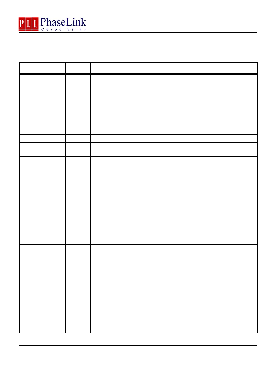
PIN DESCRIPTIONS
Name Number
Type
Description
XIN
2
I
14.318Mhz crystal input to be connected to one end of the crystal
XOUT
3
O
14.318Mhz crystal output
REF[0:1]/FS[0,2]
5,6
B
14.318Mhz Reference clock output. This pin latch FS[0,2] value at power-
up. (See Frequency Selection table). It has an internal pull down resistor.
CPUSTP#/Vtt_Pwrgd
45
I
At power-up, this pin is the input of Vtt_PWRGD After the first high to low,
this pin acts as CPU_STOP to disable all CPU clock outputs including when
Low. When Vtt_PWRGD input is high, FS (0:3), MULTSEL, HTTSEL and
MODE inputs are latched and all outputs are enabled. It has 120K ohm
internal pull up resistor.
AGP[0:1]
26,27
O
AGP clock output (see Frequency table).
HTT[C/T]_[0:1] 29,30,
33,34
O
Differential pair output for Hyper Transport output clocks
WDRESET
46
O
Watch Dog reset signal will be generated after watchdog timer expires if
I2C Enable bit (Byte9.bit7) is set active
PCI[0:4] 13,14,15,
18,19
O
PCI clock output (see Frequency table).
PCI5/HTTSEL
12
B
This pin latches the HTTSEL value at power-up. After power-up, this pin
acts as PCI clock output. HTTSEL is used to select the current multiplier for
the HTT outputs.
If HTTSEL=0, IOH=8XIREF.
If HTTSEL=1, IOH=9XIREF. It has an internal pull-up resistor.
PCI6/MULTSEL
9
B
This pin latches the MULTSEL value at power-up. After power-up, this pin
acts as PCI clock output. MULTSEL is used to select the current multiplier
for the CPU outputs.
If MULTSEL=0, IOH=6XIREF.
If MULTSEL=1, IOH=7XIREF. It has an internal pull-down resistor.
PCI7/FS1
8
B
Bi-directional pin. At power-up, the FS1 input value is latched. After power-
up, this pin acts as PCI7 output. It has an internal pull-down resistor.
PCI8//PCI_STOP#
7
B
When MODE=1 (pin23), this pin acts as PCI_STOP input to stop all PCI
clock outputs except PCIF when low. When MODE is low, this pin will acts
as PCI clock output. It has 120K ohm internal pull up resistor.
PCIF/SEL24_48#
20
B
This pin latches SEL24_48 value at power up. After power-up, this pin acts
as PCIF clock output. SEL24_48=1, select 24Mhz. SEL24_48=0 select
48Mhz. It has 120K ohm internal pull up resistor.
CPU[C/T]_0
39,40
O
Differential pair output for CPU Host.
CPU[C/T]_1
43,44
O
Differential pair output for CPU Chip Sets.
24_48MHz/MODE
23
B
This pin latches the MODE value at power-up. After power-up, this pin acts
as 24_48MHz clock output with default 24MHz or selection by I2C. MODE
function is to select mobile or desktop mode for pin 7. It has 120K ohm
internal pull up resistor.

PLL202-108
Programmable Clock Generator for ALI 1681 P4 Chip Sets
47745 Fremont Blvd., Fremont, California 94538 TEL (510) 492-0990 FAX (510) 492-0991 Rev 8/20/02 Page 3
PIN DESCRIPTIONS (Continue)
Name Number
Type
Description
48MHz/FS3
22
B
At power-up, the FS3 input value is latched. After power-up, this pin acts
as USB output. It has an internal pull-down resistor.
Iref
38
O
This pin establishes the reference current for the CPU and HTT differential
pairs, it requires a fixed precision resistor tied to ground in order to
establish the appropriate current.
SDATA
47
B
Serial data inputs for serial interface port.
SCLK
48
I
Serial data inputs for serial interface port.
VDDPCI
11,16
P
3.3V Power Supply for PCIF, PCI[0:8] clock
VDDAGP
28
P
3.3V Power Supply for AGP clock.
VDDHTT
32
P
3.3V Power Supply for HTT clock.
VDD48M
24
P
3.3V Power Supply for 48MHz and 24_48MHz clock
AVDD
36
P
3.3V power for internal PLL.
VDDCPU
42
P
3.3v power supply for CPU[T,C]_[0:1] clocks.
VDDREF
1
P
3.3v power supply for REF[0:2] clocks
VSS 4,10,17,21,2
5,31,37,41,
P Ground.
HOST SWING SELECT FUNCTIONS
MULTISEL0
Board Target
Trace/Term Z
Reference R (Rr)
I
ref
= VDD/(3*Rr)
Output Current
V
oh
@ Z
0
50
Rr = 221
; 1%
Iref = 5.0mA
I
oh
= 6*IREF
1.0V @ 50
1
50
Rr = 475
; 1%
Iref = 2.32 mA
I
oh
= 7*IREF
0.7V @ 50

PLL202-108
Programmable Clock Generator for ALI 1681 P4 Chip Sets
47745 Fremont Blvd., Fremont, California 94538 TEL (510) 492-0990 FAX (510) 492-0991 Rev 8/20/02 Page 4
FREQUENCY (MHz) SELECTION TABLE
FS4 FS3 FS2 FS1 FS0 CPU AGP HTT
PCI
SST
Amplitude
VCO
(CPU)
N
0 0 0 0 0 100.00 66.67 33.33 33.33 -0.5%
down 400 0.45 14,286
0 0 0 0 1 133.33 66.67 33.33 33.33 -0.5%
down 400 0.60 14,286
0 0 0 1 0 200.00 66.67 33.33 33.33 -0.5%
down 400 0.90 14,286
0 0 0 1 1 166.67 66.67 33.33 33.33 -0.5%
down 333 0.90 11,905
0 0 1 0 0 66.67 66.67 33.33 33.33
±0.3% center
400 0.30 14,286
0 0 1 0 1 90.00 60.00 30.00 30.00
±0.3% center
360 0.45 12,857
0 0 1 1 0 105.00 70.00 35.00 35.00
±0.3% center
420 0.45 15,000
0 0 1 1 1 165.00 55.00 27.50 27.50
±0.3% center
330 0.90 11,786
0 1 0 0 0 101.00 67.33 33.67 33.67
±0.3% center
404 0.45 14,429
0 1 0 0 1 134.67 67.33 33.67 33.67
±0.3% center
404 0.60 14,429
0 1 0 1 0 202.00 67.33 33.67 33.67
±0.3% center
404 0.90 14,429
0 1 0 1 1 168.33 67.33 33.67 33.67
±0.3% center
337 0.90 12,024
0 1 1 0 0 103.00 68.67 34.33 34.33
±0.3% center
412 0.45 14,714
0 1 1 0 1 137.33 68.67 34.33 34.33
±0.3% center
412 0.60 14,714
0 1 1 1 0 206.00 68.67 34.33 34.33
±0.3% center
412 0.90 14,714
0 1 1 1 1 171.67 68.67 34.33 34.33
±0.3% center
343 0.90 12,262
1 0 0 0 0 105.00 70.00 35.00 35.00
±0.3% center
420 0.45 15,000
1 0 0 0 1 140.00 70.00 35.00 35.00
±0.3% center
420 0.60 15,000
1 0 0 1 0 210.00 70.00 35.00 35.00
±0.3% center
420 0.90 15,000
1 0 0 1 1 175.00 70.00 35.00 35.00
±0.3% center
350 0.90 12,500
1 0 1 0 0 107.00 71.33 35.67 35.67
±0.3% center
428 0.45 15,286
1 0 1 0 1 142.67 71.33 35.67 35.67
±0.3% center
428 0.60 15,286
1 0 1 1 0 214.00 71.33 35.67 35.67
±0.3% center
428 0.90 15,286
1 0 1 1 1 178.35 71.34 35.67 35.67
±0.3% center
357 0.90 12,739
1 1 0 0 0 110.00 73.33 36.67 36.67
±0.3% center
440 0.45 15,714
1 1 0 0 1 146.67 73.33 36.67 36.67
±0.3% center
440 0.60 15,714
1 1 0 1 0 220.00 73.33 36.67 36.67
±0.3% center
440 0.90 15,714
1 1 0 1 1 183.35 73.34 36.67 36.67
±0.3% center
367 0.90 13,096
1 1 1 0 0 113.00 75.33 37.67 37.67
±0.3% center
452 0.45 16,143
1 1 1 0 1 150.67 75.33 37.67 37.67
±0.3% center
452 0.60 16,143
1 1 1 1 0 226.00 75.33 37.67 37.67
±0.3% center
452 0.90 16,143
1 1 1 1 1 188.35 75.34 37.67 37.67
±0.3% center
377 0.90 13,454
PLL202-108
Programmable Clock Generator for ALI 1681 P4 Chip Sets
47745 Fremont Blvd., Fremont, California 94538 TEL (510) 492-0990 FAX (510) 492-0991 Rev 8/20/02 Page 5
I2C BUS CONFIGURATION SETTING
Address Assignment
A6 A5 A4 A3 A2 A1 A0 R/W
1 1 0 1 0 0 1 _
Slave
Receiver/Transmitter
Provides both slave write and readback functionality
Data Transfer Rate
Standard mode at 100kbits/s
Data Protocol
This serial interface is designed to allow multiple protocols to write and read from the
controller. It includes Block Read/Write, Block Index Read/Write, Byte Read/Write and Word
Read/Write. In general, the bytes must be accessed in sequential order from lowest to highest
byte. Each byte transferred must be followed by 1 acknowledge bit. A byte transferred without
acknowledged bit will terminate the transfer. The write or read block both begins with the
master sending a slave address and a write condition (0xD2) or a read condition (0xD3).
WRITE MODE
Block
Write
S
Address
D2
A
Command
00
A
A
A
A
A
A P
Block
Index Write
S
Address
D2
A
Command M
=(00~22)
A
A
A
A
A
A P
Byte Write
S
Address
D2
A
Command M'
=(00~22)+128
A
A P
Word Write S
Address
D2
A
Command M'
=(00~22)+128
A
A
A P
READ MODE
Block
Read
S
Address
D2
A
Command
00
A S
A
A
A
A
A
Data
Byte N
A P
Block
Index Read
S
Address
D2
A
Command M
=(00~22)
A S
A
A
A
A
A
Data
Byte M+N-1
A P
Byte Read
S
Address
D2
A
Command M'
=(00~22)+128
A S
A
A P
Word Read S
Address
D2
A
Command M'
=(00~22)+128
A S
A
A
A P
Legend:
S Start
A
P Stop
Data
Byte M
Address
D3
Byte count
N
Data
--------
Data
Byte M+1
Data
Byte M
Data
Byte N
Byte count
N
Data
Byte M
Data
Byte M+1
Data
--------
Data
Byte M+N-1
Data
Byte 2
Data
--------
Byte count
N
Data
Byte 1
Address
D3
Byte count
N
Data
Byte 1
Data
Byte 2
Data
Byte M+1
Data
--------
Address
D3
Data
Byte M
Data
Byte M
Acknowledge to
host
Address
D3
Data
Byte M
Data
Byte M+1