 | –≠–ª–µ–∫—Ç—Ä–æ–Ω–Ω—ã–π –∫–æ–º–ø–æ–Ω–µ–Ω—Ç: PLL202-54 | –°–∫–∞—á–∞—Ç—å:  PDF PDF  ZIP ZIP |

PLL202-54
Programmable Clock Generator for VIA Apollo Pro-266 with VID
47745 Fremont Blvd., Fremont, California 94538 TEL (510) 492-0990 FAX (510) 492-0991 Rev 10/18/00 Page 1
FEATURES
∑
Generates all clock frequencies for
Pentium
/
system processor.
∑
Support 3 CPU clocks, 3 AGP and 9 PCI.
∑
Enhanced PCI Output Drive selectable by I2C.
∑
One 48MHz clock (or 24_48MHz clock via I2C).
∑
Three 2.5V APIC and two 14.318MHz ref. clocks.
∑
Program 5-bit CPU VID (Voltage Identification)
through I2C.
∑
Power management control to stop CPU, PCI,
AGP, and APIC clocks.
∑
Supports 2-wire I2C serial bus interface with
readback.
∑
Single byte micro-step linear Frequency
Programming via I2C with glitch free smooth
switching.
∑
Built-in programmable watchdog timer.
∑
Spread Spectrum
±
0.25% center,
±
0.5% center,
±
0.75% center, and 0 to -0.5% downspread .
∑
50% duty cycle with low jitter.
∑
Available in 300 mil 56 pin SSOP.
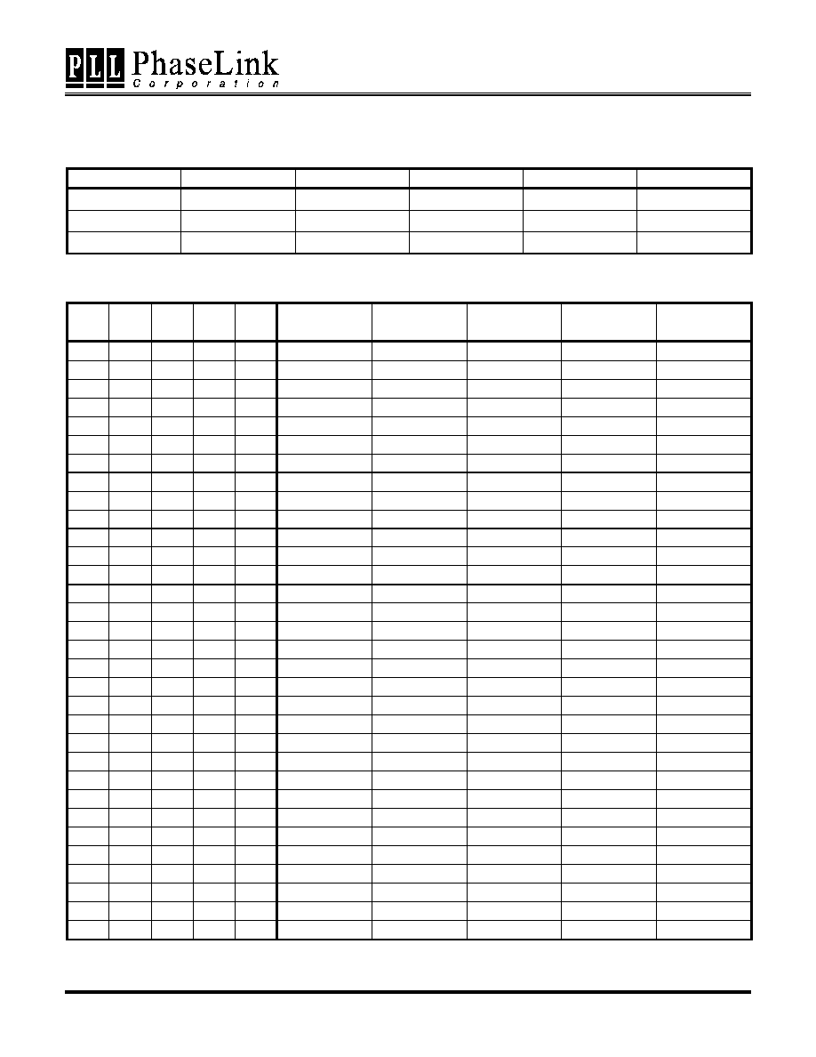
BLOCK DIAGRAM
PIN CONFIGURATION
Note: ^: Pull up #: Active low
*
: Bi-directional up latched at power-up
POWER GROUP
∑
VDD1: REF(0:1), XIN, XOUT, PLL CORE
∑
VDD2: 48MHz or 24_48MHz
∑
VDD3: PCI(0:7), PCI_F
∑
VDD4: AGP(0:2)
∑
VDD5: I2C, VID
∑
VDDL1: APIC(0:2)
∑
VDDL2: CPU(0:2)
KEY SPECIFICATIONS
∑
CPU Cycle to Cycle jitter: 250ps.
∑
PCI Cycle to Cycle jitter: 500ps.
∑
PCI to PCI skew: 500ps.
∑
CPU to CPU skew 175ps.
∑
CPU to PCI skew (CPU lead): typical 2ns.
∑
AGP to AGP skew: 250ps.
48Mhz
24_48Mhz
PD
XIN
XOUT
SDATA
SCLK
FS (0:4)*
XTAL
OSC
I2C
Logic
PLL1
SST
Control
Logic
VDD1
REF(0:1)
VDDL2
CPU (0:2)
APIC (0:2)
VDD4
AGP (0:2)
PCI (0:7)
PCI_F
VDDL1
VDD3
VDD2
PLL2
˜ 2
VID(0:4)
Registers
SDATA
SCLK
PLL202-54
PCI7
GND
PCI6
PCI5
PCI4
VDD3
PCI3
GND
PCI1
PCI_F
GND
24_48Mhz/FS2
VDD2
XOUT
XIN
GND
VDD1
VDD5
VIDENB
VDD3
AGP0
FS1
PCI0
VDDL2
GND
CPU0
CPU1
VDDL2
GND
CPU2
CPU_STOP#
PCI_STOP/WDRESET#
PD#
VDD4
REF0
REF1/FS4
VDDL1
APIC0
APIC1
GND
APIC2
GND
AGP2
SDATA
SCLK
AGP1
VID3
VID4
GND
GND
1
2
3
4
5
6
7
8
9
10
11
12
13
14
15
16
17
18
19
20
21
22
23
24
28
27
26
25
48
47
46
45
44
43
42
41
40
39
38
37
36
35
34
33
32
31
30
29
49
50
52
51
53
54
55
56
PCI2
48MHz/FS3
*
^
*
^
^
FS0
^
^
^
^
^
*
^
^
VID0
VID1
VID2
^

PLL202-54
Programmable Clock Generator for VIA Apollo Pro-266 with VID
47745 Fremont Blvd., Fremont, California 94538 TEL (510) 492-0990 FAX (510) 492-0991 Rev 10/18/00 Page 2
PIN DESCRIPTIONS
Name
Number
Type
Description
VDD1
1
P
Power supply for REF(0:1), crystal oscillator and PLL core.
VDD2
5
P
Power supply for 48MHz or 24_48MHz.
VDD3
15,24
P
Power supply for PCI(0:7), PCI_F.
VDD4
39
P
Power supply for AGP(0:2).
VDD5
31
P
Power supply for SDATA, SCLK, VID[0:4] and internal I2C Latches.
VDDL1
54
P
Power supply for APIC(0:2) (2.5V).
VDDL2
45,49
P
Power supply for CPU(0:2) (2.5V).
GND
2,8,12,19,32,33,
38,44,48,51
P
Ground.
XIN
3
I
14.318MHz crystal input to be connected to one end of the crystal.
XOUT
4
O
14.318MHz crystal output.
PD#
40
I
PD is Asynchronous active low input used to power down the device into
a low power state. The internal clocks are disabled and the VCO and the
crystal are stopped.
PCI_STOP/
WDRESET#
41
I
When input is LOW, PCI_STOP will stop PCI(0:7) except PCI_F. The
enable of the watchdog timer masks the PCI_STOP action.
CPU_STOP
42
B
When input is LOW, CPU_STOP will stop CPU(0:2).
PCI_F, PCI(0:7)
9,10,11,13,14,
16,17,18,20
O
PCI clocks with frequencies defined by Frequency Table. These pins
except PCI_F will be LOW when PCI_STOP is LOW.
CPU(0:2)
47,46,43
O
CPU clocks with frequencies defined by Frequency Table. These pins
are LOW when CPU_STOP is LOW.
AGP(0:2)
23,34,35
O
AGP clocks outputs defined as 2x PCI.
SDATA
37
B
SCLK
36
I
Serial data input for serial interface port.
VIDENB
25
I
When input is Low, it will disable the output of VID(0:4) which allows
CPU VID data directly sent to PWM. When High, it enables the override
of the CPU VID data by writing Byte5 of I2C register. This pin has 120K
internal pull up.
VID(0:4)
26,27,28,29,30
O
CPU voltage ID ouput
REF1/FS4*
48MHz/FS3*
24_48MHz/FS2*
55,6,7
B
At power up, these pins are input pins and will determine the CPU clock
frequency. After input sampling, these pins will generate output clocks.
They all have internal pull up.
FS1,FS0
21,22
I
At power up, these pins will determine the CPU clock frequency.
APIC(0:2)
53,52,50
O
2.5V APIC clock output running synchronous with PCI/2 clock output. It
is controlled by I2C byte 5 and byte 1.
REF0
56
O
3.3V 14.318MHz clock output.
PLL202-54
Programmable Clock Generator for VIA Apollo Pro-266 with VID
47745 Fremont Blvd., Fremont, California 94538 TEL (510) 492-0990 FAX (510) 492-0991 Rev 10/18/00 Page 3
POWER MANAGEMENT
CPU_STOP
PCI_SOTP
CPU(0:1)
PCI
PCI_F
XTAL,VCO
1
1
Running
Running
Running
Running
0
1
Low
Running
Running
Running
1
0
Running
Low
Running
Running
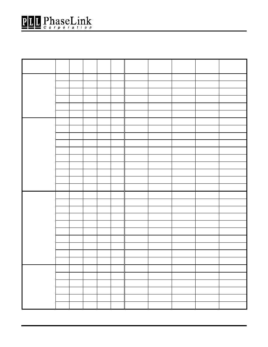
FREQUENCY (MHz) SELECTION TABLE
FS4
FS3
FS2
FS1
FS0
CPU
AGP
PCI
APIC
Spread
Spectrum
0
0
0
0
0
200.0
80.0
40.0
20.0
±
0.25%
0
0
0
0
1
190.0
76.0
38.0
19.0
±
0.25%
0
0
0
1
0
180.0
72.0
36.0
18.0
±
0.25%
0
0
0
1
1
170.0
68.0
34.0
17.0
±
0.25%
0
0
1
0
0
166.0
66.4
33.2
16.6
±
0.25%
0
0
1
0
1
160.0
64.0
32.0
13.0
±
0.25%
0
0
1
1
0
150.0
75.0
37.5
18.7
±
0.25%
0
0
1
1
1
145.0
72.5
36.2
18.1
±
0.25%
0
1
0
0
0
140.0
70.0
35.0
17.5
±
0.25%
0
1
0
0
1
136.0
68.0
34.0
17.0
±
0.25%
0
1
0
1
0
130.0
65.0
32.5
16.2
±
0.25%
0
1
0
1
1
124.0
62.0
31.0
15.5
±
0.25%
0
1
1
0
0
66.8
66.8
33.4
16.7
±
0.75%
0
1
1
0
1
100.2
66.8
33.4
16.7
±
0.75%
0
1
1
1
0
118.0
78.6
39.3
19.6
±
0.25%
0
1
1
1
1
133.4
66.7
33.3
16.6
±
0.75%
1
0
0
0
0
66.8
66.8
33.4
16.7
±
0.25%
1
0
0
0
1
100.2
66.8
33.4
16.7
±
0.25%
1
0
0
1
0
115.0
76.6
38.3
19.1
±
0.25%
1
0
0
1
1
133.4
66.7
33.3
16.6
±
0.25%
1
0
1
0
0
66.8
66.8
33.4
16.7
±
0.5%
1
0
1
0
1
100.2
66.8
33.4
16.7
±
0.5%
1
0
1
1
0
110.0
73.3
36.6
18.3
±
0.25%
1
0
1
1
1
133.4
66.7
33.3
16.6
±
0.5%
1
1
0
0
0
105.0
70.0
35.0
17.5
±
0.25%
1
1
0
0
1
90.0
60.0
30.0
15.0
±
0.25%
1
1
0
1
0
85.0
56.6
28.3
14.1
±
0.25%
1
1
0
1
1
78.0
78.0
39.0
19.5
±
0.25%
1
1
1
0
0
66.6
66.6
33.3
16.6
0 to- 0.5%
1
1
1
0
1
100.0
66.6
33.3
16.6
0 to- 0.5%
1
1
1
1
0
75.0
75.0
37.5
18.7
±
0.25%
1
1
1
1
1
133.3
66.6
33.3
16.6
0 to- 0.5%
PLL202-54
Programmable Clock Generator for VIA Apollo Pro-266 with VID
47745 Fremont Blvd., Fremont, California 94538 TEL (510) 492-0990 FAX (510) 492-0991 Rev 10/18/00 Page 4
FREQUENCY (MHz) SELECTION TABLE BY GROUP TIMING
Divider Ratio
(CPU:AGP)
FS4
FS3
FS2
FS1
FS0
CPU
AGP
PCI
APIC
Spread
Spectrum
1
1
1
0
0
66.6
66.6
33.3
16.6
0 to- 0.5%
0
1
1
0
0
66.8
66.8
33.4
16.7
±
0.75%
1
0
0
0
0
66.8
66.8
33.4
16.7
±
0.25%
1
0
1
0
0
66.8
66.8
33.4
16.7
±
0.5%
1
1
1
1
0
75.0
75.0
37.5
18.7
±
0.25%
A
(1 : 1)
1
1
0
1
1
78.0
78.0
39.0
19.5
±
0.25%
1
1
0
1
0
85.0
56.6
28.3
14.1
±
0.25%
1
1
0
0
1
90.0
60.0
30.0
15.0
±
0.25%
1
1
1
0
1
100.0
66.6
33.3
16.6
0 to- 0.5%
0
1
1
0
1
100.2
66.8
33.4
16.7
±
0.75%
1
0
0
0
1
100.2
66.8
33.4
16.7
±
0.25%
1
0
1
0
1
100.2
66.8
33.4
16.7
±
0.5%
1
1
0
0
0
105.0
70.0
35.0
17.5
±
0.25%
1
0
1
1
0
110.0
73.3
36.6
18.3
±
0.25%
1
0
0
1
0
115.0
76.6
38.3
19.1
±
0.25%
B
(1.5 : 1)
0
1
1
1
0
118.0
78.6
39.3
19.6
±
0.25%
0
1
0
1
1
124.0
62.0
31.0
15.5
±
0.25%
0
1
0
1
0
130.0
65.0
32.5
16.2
±
0.25%
1
1
1
1
1
133.3
66.6
33.3
16.6
0 to- 0.5%
0
1
1
1
1
133.4
66.7
33.3
16.6
±
0.75%
1
0
0
1
1
133.4
66.7
33.3
16.6
±
0.25%
1
0
1
1
1
133.4
66.7
33.3
16.6
±
0.5%
0
1
0
0
1
136.0
68.0
34.0
17.0
±
0.25%
0
1
0
0
0
140.0
70.0
35.0
17.5
±
0.25%
0
0
1
1
1
145.0
72.5
36.2
18.1
±
0.25%
C
(2 : 1)
0
0
1
1
0
150.0
75.0
37.5
18.7
±
0.25%
0
0
1
0
1
160.0
64.0
32.0
13.0
±
0.25%
0
0
1
0
0
166.0
66.4
33.2
16.6
±
0.25%
0
0
0
1
1
170.0
68.0
34.0
17.0
±
0.25%
0
0
0
1
0
180.0
72.0
36.0
18.0
±
0.25%
0
0
0
0
1
190.0
76.0
38.0
19.0
±
0.25%
D
(2.5 : 1)
0
0
0
0
0
200.0
80.0
40.0
20.0
±
0.25%

PLL202-54
Programmable Clock Generator for VIA Apollo Pro-266 with VID
47745 Fremont Blvd., Fremont, California 94538 TEL (510) 492-0990 FAX (510) 492-0991 Rev 10/18/00 Page 5
I2C BUS CONFIGURATION SETTING
Address Assignment
A6 A5 A4 A3 A2 A1 A0 R/W
1 1 0 1 0 0 1 _
Slave
Receiver/Transmitter
Provides both slave write and readback functionality
Data Transfer Rate
Standard mode at 100kbits/s
Serial Bits Reading
The serial bits will be read or sent by the clock driver in the following order
Byte 0 ≠ Bits 7, 6, 5, 4, 3, 2, 1, 0
Byte 1 ≠ Bits 7, 6, 5, 4, 3, 2, 1, 0
-
Byte N ≠ Bits 7, 6, 5, 4, 3, 2, 1, 0
Data Protocol
This serial protocol is designed to allow both blocks write and read from the controller. The
bytes must be accessed in sequential order from lowest to highest byte. Each byte transferred
must be followed by 1 acknowledge bit. A byte transferred without acknowledged bit will
terminate the transfer. The write or read block both begins with the master sending a slave
address and a write condition (0xD2) or a read condition (0xD3).
Following the acknowledge of this address byte, in
Write Mode: the Command Byte and Byte
Count Byte must be sent by the master but ignored by the slave, in Read Mode: the Byte
Count Byte will be read by the master then all other Data Byte.
I2C CONTROL REGISTERS
1. BYTE 0: Functional and Frequency Select Clock Register (1=Enable, 0=Disable)
Bit
Pin#
Default
Description
Bit 7
6
0
FS3 ( see Frequency selection Table )
Bit 6
7
0
FS2 ( see Frequency selection Table )
Bit 5
21
0
FS1 ( see Frequency selection Table )
Bit 4
22
0
FS0 ( see Frequency selection Table )
Bit 3
-
0
Frequency selection control bit 1=Via I2C, 0=Via External jumper
Bit 2
55
0
FS4 ( see Frequency selection Table )
Bit 1
-
1
0 = OFF, 1 = Spread Spectrum Enable
Bit 0
-
0
0 = Normal, 1 = Tristate Mode for all outputs