 | –≠–ª–µ–∫—Ç—Ä–æ–Ω–Ω—ã–π –∫–æ–º–ø–æ–Ω–µ–Ω—Ç: PLL205-16 | –°–∫–∞—á–∞—Ç—å:  PDF PDF  ZIP ZIP |

Preliminary
PLL205-16
Programmable Clock Generator for VIA KT-266 Chipset
47745 Fremont Blvd., Fremont, California 94538 TEL (510) 492-0990 FAX (510) 492-0991 Rev 11/21/01 Page 1
FEATURES
∑
Generates all clock frequencies for VIA KT266
chipset.
∑
Support one pair of differential CPU clocks, one
pair of differential push-pull CPU clocks, 3 AGP
and 10 PCI.
∑
Enhanced PCI Output Drive selectable by I2C.
∑
One 48MHz clock and 24_48MHz clock via I2C.
∑
Three 14.318MHz reference clocks.
∑
Power management control to stop CPU, PCI,
REF, 24_48MHz, 48MHz and AGP clocks.
∑
Supports 2-wire I2C serial bus interface with
readback.
∑
Single byte micro-step linear Frequency
Programming via I2C with glitch free smooth
switching.
∑
Built-in programmable watchdog timer up to 63
seconds with 1-second interval. It will generate a
low reset output when timer expired.
∑
Spread Spectrum
±
0.25% center,
±
0.5% center,
±
0.75% center, and 0 to -0.5% downspread.
∑
50% duty cycle with low jitter.
∑
Available in 300 mil 48 Pin SSOP.
BLOCK DIAGRAM
PIN CONFIGURATION
Note: ^: 100k internal Pull up v: 100k internal Pull down
#: Active low
*
: Bi-directional up latched at power-up
POWER GROUP
∑
VDD1: REF(0:1), REF_F, XIN, XOUT
∑
VDD2: 48MHz or 24_48MHz
∑
VDD3: PCI(0:8), PCI9_E
∑
VDD4: AGP(0:2)
∑
VDDL1: CPUT0, CPUC0, CPUT_CS, CPUC_CS
∑
VDDL2: PLL Core
KEY SPECIFICATIONS
∑
CPU Cycle to Cycle jitter: 250ps.
∑
PCI Cycle to Cycle jitter: 500ps.
∑
PCI to PCI skew: 500ps.
∑
CPU to CPU skew: 175ps.
∑
AGP to AGP skew: 250ps.
48MHz
24_48MHz
PD
XIN
XOUT
FS (0:4)*
XTAL
OSC
PLL1
SST
Control
Logic
VDD1
REF(0:1)
VDD4
AGP (0:2)
PCI (0:8)
PCI9_E
VDD3
VDD2
PLL2
˜ 2
REF_F
CPUT0
CPUC0
CPUT_CS
CPUC_CS
VDDL1
SDATA
SCLK
I2C
Logic
Watch
Dog
WDRESET#
CPUC0
VDDL1
CPUT_CS
CPUC_CS
GND
CPU_STOP#^
PCI_STOP#^
PD#^
VDDL2
GND
SDATA
VDD3
1
2
3
4
5
6
7
8
9
10
11
12
13
14
15
16
17
18
19
20
21
22
23
24
PLL205-16
REF0/FS0*^
REF1/FS1*^
REF_F
N/C
AGP_STOP#^
GND
CPUT0
SCLK
GND
AGP2
AGP1
AGP0
VDD4
WDRESET#^
PCI4
VDD3
PCI3
SEL24_48#^/PCI0
FS4*^/PCI_F
GND
24_48MHz/FS3*
^
48MHz/FS2*^
VDD2
XOUT
XIN
GND
VDD1
48
47
46
45
44
43
42
41
40
39
38
37
36
35
34
33
32
31
30
29
28
27
26
25
PCI1
GND
PCI2
PCI8
PCI7
GND
PCI6
PCI5
PCI9_E/SELPCI9_E*^

Preliminary
PLL205-16
Programmable Clock Generator for VIA KT-266 Chipset
47745 Fremont Blvd., Fremont, California 94538 TEL (510) 492-0990 FAX (510) 492-0991 Rev 11/21/01 Page 2
PIN DESCRIPTION
Name
Number
Type
Description
VDD1
1
P
Power supply for REF(0:1), REF_F and crystal oscillator.
VDD2
5
P
Power supply for 48MHz or 24_48MHz.
VDD3
15,23
P
Power supply for PCI(0:8), PCI9_E.
VDD4
25
P
Power supply for AGP(0:2).
VDDL1
40
P
Power supply for CPUT0, CPUC0, CPUT_CS and CPUC_CS.
VDDL2
33
P
Power supply for PLL CORE.
GND
2,8,12,19,29,
32,37,43
P
Ground.
XIN
3
I
14.318MHz crystal input to be connected to one end of the crystal.
XOUT
4
O
14.318MHz crystal output.
PD#
34
I
PD is Asynchronous active low input used to power down the device
into a low power state. The internal clocks are disabled and the VCO
and the crystal are stopped.
PCI_STOP#
35
I
When input is Low, it will stop PCI(0:8) and PCI9_E. The enable of the
watchdog timer masks the PCI_STOP action.
CPU_STOP
36
I
When input is Low, it will disable CPUT0, CPUC0, CPUT_CS and
CPUC_CS.
AGP_STOP
44
I
When input is Low, it will stop AGP(0:2).
N/C
45
Not connected
PCI(0:8)
10,11,13,14,
16,17,18,20,21
O
PCI clocks with frequencies defined by Frequency Table. These pins
will be LOW when PCI_STOP is LOW.
SEL24_48#/PCI0
10
B
PCI clock output. This pin also serves as the select 24MHz (when High)
or 48MHz (when Low) for pin7.
PCI9_E/SELPCI9_E
22
B
At power up, this pin is an input pin and will determine the operating
frequency of PCI9_E output. After input sampling, this pin will generate
PCI output clock. If SELPCI9_E=1, PCI9_E will arrive 2 ns earlier than
other PCI clocks, if SELPCI9_E=0, PCI9_E will be normal PCI output
like other PCI clock outputs.

Preliminary
PLL205-16
Programmable Clock Generator for VIA KT-266 Chipset
47745 Fremont Blvd., Fremont, California 94538 TEL (510) 492-0990 FAX (510) 492-0991 Rev 11/21/01 Page 3
PIN DESCRIPTIONS (continued)
Name
Number
Type
Description
FS4*/PCI_F
9
B
Free running PCI clock. This pin also serves as the select strap to
determine device operating frequency.
CPUT0
42
O
True clock of differential pair open drain CPU outputs. This output will
be disabled when CPU_STOP is low.
CPUC0
41
O
Complementary clock of differential pair open drain CPU outputs. This
output will be disabled when CPU_STOP is low.
CPUT_CS,
CPUC_CS
39,38
O
Differential CPU clock outputs for the chipset. They are push-pull
outputs. These outputs will be disabled when CPU_STOP is low.
AGP(0:2)
26,27,28
O
AGP clocks outputs defined as 2x PCI.
SDATA
31
B
SCLK
30
I
Serial data input for serial interface port.
REF0/FS0*
REF1/FS1*
48MHz/FS2*
24_48MHz/FS3*
FS4*/PCI_F
48,47,6,7,9
B
At power up, these pins are input pins. After input sampling, these pins
will generate output clocks. FS(0:4) have internal pull-up resistor.
WDRESET#
24
I
This pin is an open drain output. Will be Low at watchdog timer
expiration.
REF(0:1),REF_F
48,47,46
O
3.3V 14.318MHz clock output.

Preliminary
PLL205-16
Programmable Clock Generator for VIA KT-266 Chipset
47745 Fremont Blvd., Fremont, California 94538 TEL (510) 492-0990 FAX (510) 492-0991 Rev 11/21/01 Page 4
POWER MANAGEMENT
CPU_STOP PCI_STOP CPUT_CS CPUC_CS
CPUT0
CPUC0
PCI
PCI_F
XTAL,VCO
1
1
Running
Running
Running
Running
Running
Running
Running
0
1
Stopped
Low
Stopped
High
Stopped
High
Stopped
Low
Running
Running
Running
1
0
Running
Running
Running
Running
Stopped
Low
Running
Running
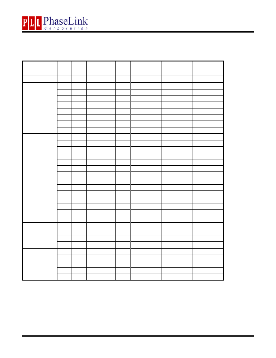
FREQUENCY (MHz) SELECTION TABLE
FS4 FS3 FS2 FS1 FS0
CPU
AGP
PCI
Spread
Spectrum
0
0
0
0
0
156
78
39
±
0.25%
0
0
0
0
1
154
77
38.5
±
0.25%
0
0
0
1
0
152
76
38
±
0.25%
0
0
0
1
1
147
73.5
36.8
±
0.25%
0
0
1
0
0
144
72
36
±
0.25%
0
0
1
0
1
142
71
35.5
±
0.25%
0
0
1
1
0
138
69
34.5
±
0.25%
0
0
1
1
1
136
68
34
±
0.25%
0
1
0
0
0
124
62
31
±
0.25%
0
1
0
0
1
122
61
30.5
±
0.25%
0
1
0
1
0
117
78
39
±
0.25%
0
1
0
1
1
115
76.7
38.3
±
0.25%
0
1
1
0
0
113
75.3
37.7
±
0.25%
0
1
1
0
1
108
72
36
±
0.25%
0
1
1
1
0
105
70
35
±
0.25%
0
1
1
1
1
102
68
34
±
0.25%
1
0
0
0
0
233.3
77.78
38.88
±
0.25%
1
0
0
0
1
220
73.3
36.6
±
0.5%
1
0
0
1
0
210
70
35
±
0.75%
1
0
0
1
1
200
66.6
33.3
±
0.25%
1
0
1
0
0
190
76
38
±
0.25%
1
0
1
0
1
180
72
36
±
0.25%
1
0
1
1
0
170
68
34
±
0.25%
1
0
1
1
1
150
75
37.5
±
0.25%
1
1
0
0
0
140
70
35
±
0.25%
1
1
0
0
1
120
60
30
±
0.25%
1
1
0
1
0
110
73.3
36.67
±
0.25%
1
1
0
1
1
66.6
66.6
33.3
±
0.25%
1
1
1
0
0
200
66.6
33.3
±
0.25%
1
1
1
0
1
166.6
66.64
33.32
±
0.25%
1
1
1
1
0
100
66.67
33.33
±
0.5%
1
1
1
1
1
133.33
66.67
33.33
±
0.75%
Preliminary
PLL205-16
Programmable Clock Generator for VIA KT-266 Chipset
47745 Fremont Blvd., Fremont, California 94538 TEL (510) 492-0990 FAX (510) 492-0991 Rev 11/21/01 Page 5
FREQUENCY (MHz) SELECTION TABLE BY GROUP TIMING
Divider Ratio
(CPU:AGP)
FS4 FS3 FS2 FS1 FS0
CPU
AGP
PCI
A ( 1: 1 )
1
1
0
1
1
66.6
66.6
33.3
1
1
1
1
0
100
66.67
33.33
0
1
1
1
1
102
68
34
0
1
1
1
0
105
70
35
0
1
1
0
1
108
72
36
1
1
0
1
0
110
73.3
36.67
0
1
1
0
0
113
75.3
37.7
0
1
0
1
1
115
76.7
38.3
B (1.5 : 1 )
0
1
0
1
0
117
78
39
1
1
0
0
1
120
60
30
0
1
0
0
1
122
61
30.5
0
1
0
0
0
124
62
31
1
1
1
1
1
133.33
66.67
33.33
0
0
1
1
1
136
68
34
0
0
1
1
0
138
69
34.5
1
1
0
0
0
140
70
35
0
0
1
0
1
142
71
35.5
0
0
1
0
0
144
72
36
0
0
0
1
1
147
73.5
36.8
1
0
1
1
1
150
75
37.5
0
0
0
1
0
152
76
38
0
0
0
0
1
154
77
38.5
B ( 2 : 1 )
0
0
0
0
0
156
78
39
1
1
1
0
1
166.6
66.64
33.32
1
0
1
1
0
170
68
34
1
0
1
0
1
180
72
36
C ( 2.5 : 1 )
1
0
1
0
0
190
76
38
1
1
1
0
0
200
66.6
33.3
1
0
0
1
1
200
66.6
33.3
1
0
0
1
0
210
70
35
1
0
0
0
1
220
73.3
36.6
D ( 3 : 1 )
1
0
0
0
0
233.3
77.78
38.88