 | –≠–ª–µ–∫—Ç—Ä–æ–Ω–Ω—ã–π –∫–æ–º–ø–æ–Ω–µ–Ω—Ç: PLL501-05 | –°–∫–∞—á–∞—Ç—å:  PDF PDF  ZIP ZIP |
PLL501-05/-07
VCXO Clock Generator IC
47745 Fremont Blvd., Fremont, California 94538 TEL (510) 492-0990 FAX (510) 492-0991 Rev 05/10/01 Page 1
FEATURES
∑
Integrated voltage-controlled crystal oscillator
circuitry (VCXO) (pull range 200ppm minimum).
∑
Ideal for ADSL (35.328MHz and 70.656MHz).
∑
VCXO tuning range: 0 - 3.3V.
∑
Integrated phase-locked loop (PLL) provides
pullable output at 35.328MHz (for PLL501-05)
and 70.656MHz (for PLL501-07) with a
13.248MHz low cost parallel resonant crystal.
∑
Accepts fundamental-mode parallel resonant
crystals from 8 to 15 MHz.
∑
3.3V supply voltage.
∑
Small circuit board footprint (8-pin 0.150'' SOIC).
∑
12mA output drives capability at TTL level.
DESCRIPTIONS
The PLL501-05 and PLL501-07 are monolithic low
jitter, high performance CMOS VCXO chips. They
allow the control of the output frequency with an
input voltage (VIN), using a low cost crystal.
The PLL501-05 and PLL501-07 are ideal for ADSL
applications. With a low cost 13.248MHz crystal, the
PLL501-05 provides a pullable 35.328MHz output
clock, while the PLL501-07 provides a 70.656MHz
output clock.
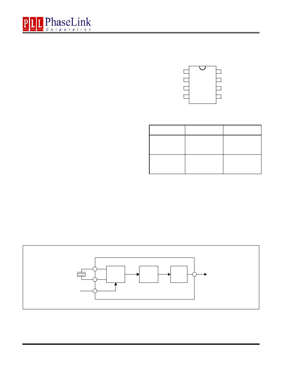
PIN CONFIGURATION
Table 1: Crystal / Output Frequencies
DEVICE
F
XIN
(MHz)
CLK (MHz)
PLL501-05
13.248
(8 to 15)
35.328
(2.667 x F
XIN
)
PLL501-07
13.248
(8 to 15)
70.656
(5.333 x F
XIN
)
Note: Contact PhaseLink for custom PLL Frequencies
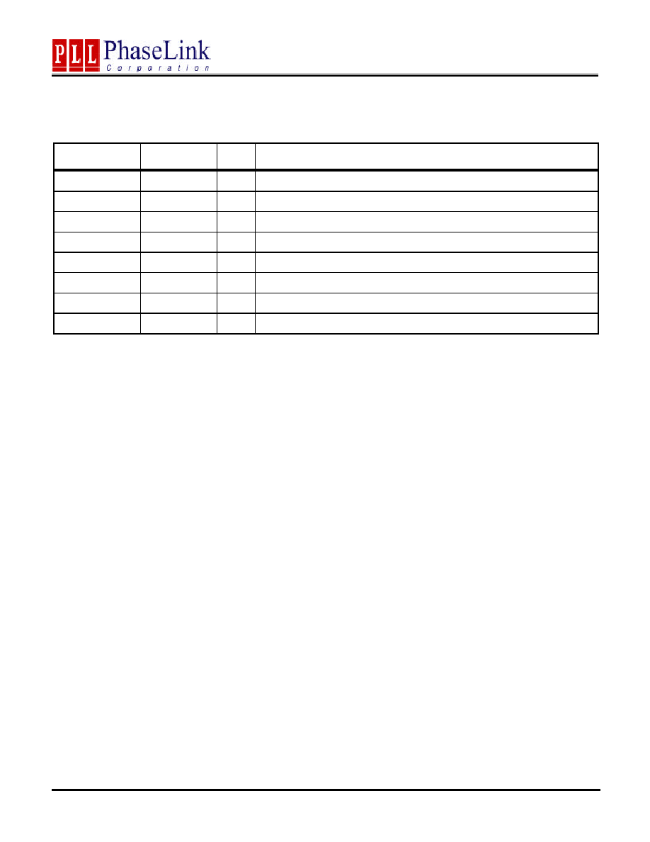
BLOCK DIAGRAM
VIN
XOUT
XIN
VCXO
PLL
CLK
Output
Buffer
PLL501-XX
1
2
3
4
5
6
7
8
XIN
VDD
VIN
GND
XOUT
VDD
CLK
GND
PLL501-05/-07
VCXO Clock Generator IC
47745 Fremont Blvd., Fremont, California 94538 TEL (510) 492-0990 FAX (510) 492-0991 Rev 05/10/01 Page 2
PIN DESCRIPTIONS
Name
Number
Type
Description
XIN
1
I
Crystal input connection (parallel resonant crystal, C
L
= 10pF).
VDD
2
P
3.3V Power Supply.
VIN
3
I
Voltage Input for VCXO Frequency Control.
GND
4
P
Ground for PLL Core.
CLK
5
O
Clock Output.
VDD
6
P
3.3V Power Supply.
GND
7
P
Ground.
XOUT
8
O
Crystal connection.
PLL501-05/-07
VCXO Clock Generator IC
47745 Fremont Blvd., Fremont, California 94538 TEL (510) 492-0990 FAX (510) 492-0991 Rev 05/10/01 Page 3
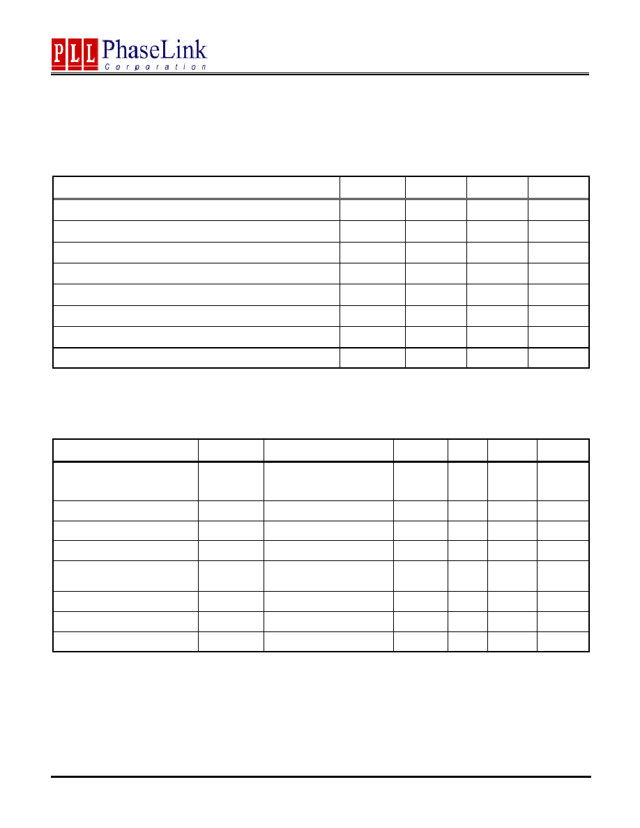
ELECTRICAL SPECIFICATIONS
1. Absolute Maximum Ratings
PARAMETERS
SYMBOL
MIN.
MAX.
UNITS
Supply Voltage
V
DD
7
V
Input Voltage, dc
V
I
V
SS
-
0.5
V
DD
+
0.5
V
Output Voltage, dc
V
O
V
SS
-
0.5
V
DD
+
0.5
V
Storage Temperature
T
S
-65
150
∞
C
Ambient Operating Temperature
T
A
0
70
∞
C
Junction Temperature
T
J
125
∞
C
Lead Temperature (soldering, 10s)
260
∞
C
Input Static Discharge Voltage Protection
2
kV
Exposure of the device under conditions beyond the limits specified by Maximum Ratings for extended periods may cause permanent damage to the
device and affect product reliability. These conditions represent a stress rating only, and functional operations of the device at these or any other
conditions above the operational limits noted in this specification is not implied.
2. DC Electrical Specifications
PARAMETERS
SYMBOL
CONDITIONS
MIN.
TYP.
MAX.
UNITS
Supply Current, Dynamic, with
Loaded Outputs
I
DD
F
XIN
= 8 - 15MHz
Ouput load of 10pF
20
mA
Operating Voltage
V
DD
3.13
3.47
V
Output High Voltage
V
OH
I
OH
= -12mA
2.4
V
Output Low Voltage
V
OL
I
LO
= 12mA
0.4
V
Output High Voltage at CMOS
level
V
OHC
I
OH
= -4mA
V
DD
≠ 0.4
V
Operating Supply Current
I
DD
No Load
7
mA
Short Circuit Current
±
50
mA
VIN, VCXO Control Voltage
0
3.3
V
PLL501-05/-07
VCXO Clock Generator IC
47745 Fremont Blvd., Fremont, California 94538 TEL (510) 492-0990 FAX (510) 492-0991 Rev 05/10/01 Page 4
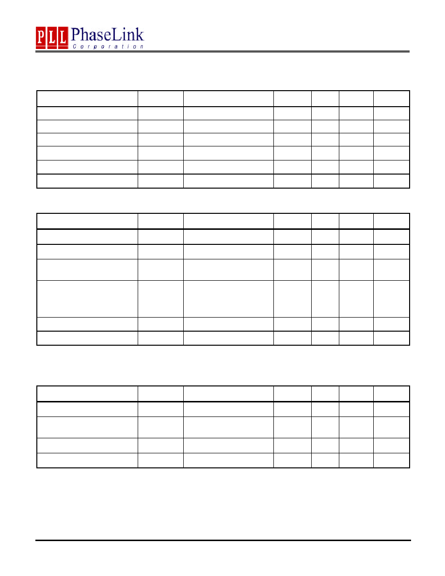
3. AC Electrical Specifications
PARAMETERS
SYMBOL
CONDITIONS
MIN.
TYP.
MAX.
UNITS
Input Crystal Frequency
8
15
MHz
Output Clock Rise Time
t
r
0.8V ~ 2.0V
1.5
ns
Output Clock Fall Time
t
f
2.0V ~ 0.8V
1.5
ns
Output Clock Duty Cycle
Measured @ 1.4V
45
50
55
%
Max Absolute Jitter
Short Term
100
ps
Short Circuit Current
±
50
mA
4. Voltage Control Crystal Oscillator
PARAMETERS
SYMBOL
CONDITIONS
MIN.
TYP.
MAX.
UNITS
PLL Stabilization Time *
T
PLLSTB
From VCXO stable
500
µ
s
VCXO Stabilization Time *
T
VCXOSTB
From power valid
10
ms
Output Frequency Synthesis
Error
(Unless otherwise noted in
Frequency Table)
±
30
ppm
VCXO Tuning Range
F
XIN
= 8 - 15MHz;
XTAL C
0
/C
1
< 250;
C
L
=10pF
200
ppm
CLK output pullability
0V
VIN
3.3V
±
100
ppm
VCXO Tuning Characteristic
100
ppm/V
Note: Parameters denoted with an asterisk ( * ) represent nominal characterization data and are not production tested to any specific limits.
5. Crystal Specifications
PARAMETERS
SYMBOL
CONDITIONS
MIN.
TYP.
MAX.
UNITS
Crystal Resonator Frequency
F
XIN
Parallel Fundamental Mode
8
15
MHz
Crystal Loading Capacitance
Rating
C
L
(xtal)
10
pF
Crystal Pullability
C
0
/C
1
(xtal)
At cut
250
-
Recommended ESR
R
E
At cut
30

PLL501-05/-07
VCXO Clock Generator IC
47745 Fremont Blvd., Fremont, California 94538 TEL (510) 492-0990 FAX (510) 492-0991 Rev 05/10/01 Page 5
6. External Components and Layout Recommendations
The PLL501-05/-07 requires a minimum number of external components for proper operation. A
standard low frequency decoupling capacitor of 2
µ
F or more should be used between VDD and GND
(pin 2 and pin 4, as well as pin 6 and pin 7). Additionally, higher frequency decoupling capacitors of
0.01
µ
F are required between VDD and GND (between pin 2 and 4, and between pin 6 and 7). These
higher frequency decoupling capacitors must be connected as close to the PLL501-05/-07 chip as
possible, and preferably directly next to the PLL501-05/-07 pins. A series termination resistor of 33
may be used for the clock output.
The input crystal must be connected as close to the chip as possible, and preferably directly next to the
PLL501-05/-07 pins.
If a crystal with C
L
higher than 10pF is used, it will requires additional loading capacitors
externally to complement the internal 10pF of the PLL501-05/-07:
one between each crystal electrode and
GND, as close to the crystal as possible, and preferably directly next to the crystal electrodes. Consult
PhaseLink for recommended suppliers.
PLL501-05/-07
VCXO Clock Generator IC
47745 Fremont Blvd., Fremont, California 94538 TEL (510) 492-0990 FAX (510) 492-0991 Rev 05/10/01 Page 6
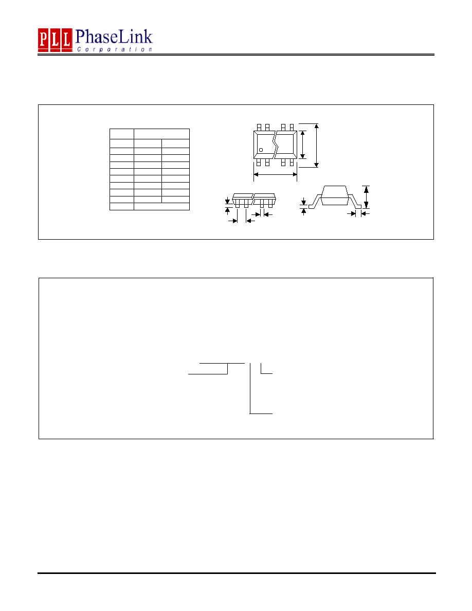
PACKAGE INFORMATION
ORDERING INFORMATION
PhaseLink Corporation, reserves the right to make changes in its products or specifications, or both at any time without notice. The information
furnished by Phaselink is believed to be accurate and reliable. However, PhaseLink makes no guarantee or warranty concerning the accuracy of said
information and shall not be responsible for any loss or damage of whatever nature resulting from the use of, or reliance upon this product.
LIFE SUPPORT POLICY: PhaseLink's products are not authorized for use as critical components in life support devices or systems without the
express written approval of the President of PhaseLink Corporation.
For part ordering, please contact our Sales Department:
47745 Fremont Blvd., Fremont, CA 94538, USA
Tel: (510) 492-0990 Fax: (510) 492-0991
PART NUMBER
The order number for this device is a combination of the following:
Device number, Package type and Operating temperature range
PLL501-0x S C
PART NUMBER
TEMPERATURATRE
C=COMMERCIAL
M=MILITARY
I=INDUSTRAL
PACKAGE TYPE
S=SOIC
C
L
A
8 PIN Narrow SOIC ( mm )
SOIC
Symbol
Min.
Max.
A
1.55
1.73
A1
0.15
0.18
B
0.35
0.49
C
0.19
0.25
D
4.80
4.98
E
3.81
3.99
H
5.84
6.20
L
0.41
0.89
e
1.27 BSC
E
H
D
A
1
e
B