Preliminary
PLL501-22
27MHz Multiple Output VCXO with Audio Clock
47745 Fremont Blvd., Fremont, California 94538 TEL (510) 492-0990 FAX (510) 492-0991 Rev 02/26/04 Page 1
FEATURES
∑ 2 VCXO outputs at 27MHz (27MHz crystal input).
∑ Selectable Audio Clocks supporting:
32kHz, 44.1kHz, 48kHz, 64kHz and 96kHz
sampling rates
256, 384 and 512 oversampling ratios
8.192, 11.2896, 12.288, 16.9344, 16.384,
18.432, 22.5792, 24.576MHz audio frequencies
∑ +/- 120ppm pull range
∑ Power down tri-state selector.
∑ 3.3V Operating Voltage.
∑ No external load capacitor or varicap required.
∑ Available in 16-Pin SSOP.
DESCRIPTION
The PLL501-22 is a low cost integrated VCXO IC with
power down feature, designed to work with a
fundamental 27MHz crystal in order to provide most
common audio clocks (8.192, 11.2896, 12.288,
16.9344, 16.384, 18.432, 22.5792, and 24.576MHz)
required by sampling rates of 32kHz, 44.1kHz, 48kHz,
64kHz and 96kHz (256, 384 and 512 oversampling
ratios). The audio clock follows the pulled 27MHz
signal of the VCXO. The wide pull-range makes it
ideal for STB and MPEG Video applications.
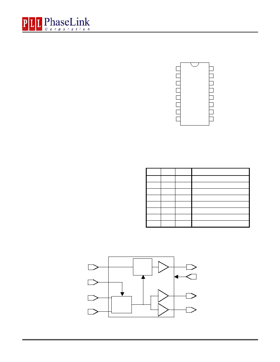
PACKAGE PIN CONFIGURATION
Note: ^: Internal pull-up resistor. The internal pull-up resistor
results in a default high value when no pull-down resistor is
connected to this pin.
AUDIO CLOCK SELECTION
S2 S1 S0
ACLK (MHz)
0 0 0
8.192
0 0 1
11.2896
0 1 0
12.288
0 1 1
16.9344
1 0 0
18.432
1 0 1
16.384
1 1 0
22.5792
1 1 1
24.576
BLOCK DIAGRAM
PLL 50
1-
2
2
1
2
3
4
5
6
7
8
XIN
9
10
11
12
13
14
15
16
XOUT
VDD
VDD
VIN
GND
GND
PDOWN^
S1^
27MHz
VDD
S0^
27MHz
GND
ACLK
S2^
XIN = 27 MHz
Xout
PDOWN
27MHz
Xin
[S2-S0]
Audio
PLL
VCXO
Vin
ACLK
27MHz
Preliminary
PLL501-22
27MHz Multiple Output VCXO with Audio Clock
47745 Fremont Blvd., Fremont, California 94538 TEL (510) 492-0990 FAX (510) 492-0991 Rev 03/02/04 Page 2
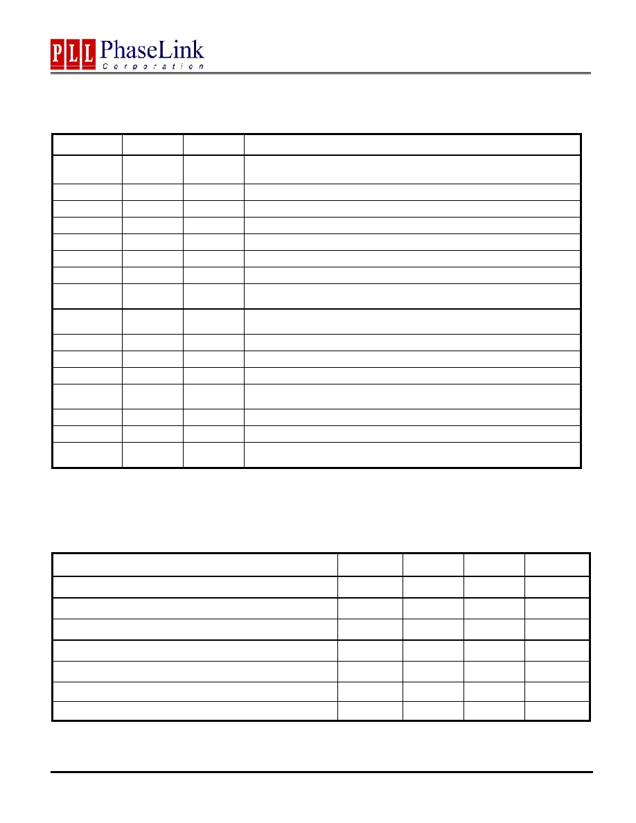
PIN DESCRIPTIONS
Name Pin
# Type
Description
XIN 1 I
Crystal input to be connected to fundamental parallel mode crystal.
(C
L
=9.5pF).
XOUT 2 I
Crystal
output
connector.
VDD 3 P
3.3V
power
supply.
VDD 4 P
3.3V
power
supply.
VIN 5
I
Frequency control input (0V to 3.3V).
GND 6 P
Ground.
GND 7 P
Ground.
PDOWN 8
I
Digital control input. This input powers down the entire chip and tri-states
all outputs when low. 60k
internal pull-up.
S2 9 I
Digital control input to select audio frequency.
60k
internal pull-up.
ACLK
10
O
Audio clock output (see selection table on page 1).
GND 11 P
Ground.
27MHz 12 O
27MHz
VCXO
output.
S0 13 I
Digital control input to select audio frequency.
60k
internal pull-up.
VDD 14 P
3.3V
power
supply.
27MHz 15 O
27MHz
VCXO
output.
S1 16 I
Digital control input to select audio frequency.
60k
internal pull-up.
Notes: I ≠ input pin; P ≠ power supply/ground pin; O ≠ output pin.
ELECTRICAL SPECIFICATIONS
1. Absolute Maximum Ratings
PARAMETERS SYMBOL
MIN.
MAX.
UNITS
Supply Voltage
V
DD
7 V
Input Voltage, dc
V
I
V
SS
-
0.5 V
DD
+
0.5
V
Output Voltage, dc
V
O
V
SS
-
0.5 V
DD
+
0.5
V
Storage Temperature
T
S
-65 150
∞C
Junction Temperature
T
J
125
∞C
Lead Temperature (soldering, 10s)
260
∞C
Input Static Discharge Voltage Protection
2
kV
Exposure of the device under conditions beyond the limits specified by Maximum Ratings for extended periods may cause permanent damage to the
device and affect product reliability. These conditions represent a stress rating only, and functional operations of the device at these or any other
conditions above the operational limits noted in this specification is not implied.

Preliminary
PLL501-22
27MHz Multiple Output VCXO with Audio Clock
47745 Fremont Blvd., Fremont, California 94538 TEL (510) 492-0990 FAX (510) 492-0991 Rev 03/02/04 Page 3
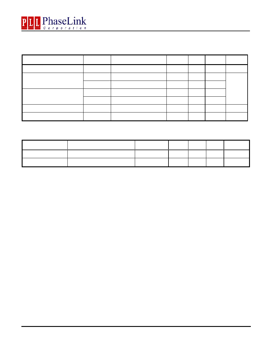
2. Crystal Specifications
PARAMETERS SYMBOL CONDITIONS MIN.
TYP.
MAX.
UNITS
Crystal Resonator Frequency
F
XIN
Parallel Fundamental Mode
27
MHz
Crystal Loading Rating
C
L
(xtal)
At VCON = 1.65V
9.5
pF
Crystal Pullability
C
0
/C
1
(xtal)
AT cut
250 -
Recommended ESR
R
E
AT cut
30
Note: Crystal Loading rating: 9.5pF is the loading the crystal sees from the VCXO chip at VCON = 1.65V. It is assumed that the crystal will be at
nominal frequency at this load. If the crystal requires more load to be at nominal frequency, the additional load must be added externally. This however
may reduce the pull range.
3. Voltage Control Crystal Oscillator
PARAMETERS SYMBOL CONDITIONS MIN.
TYP.
MAX.
UNITS
VCXO Stabilization Time *
T
VCXOSTB
From power valid
10
ms
VCXO Tuning Range
XTAL C
0
/C
1
< 250
240
ppm
CLK output pullability
0V
VCON 3.3V
±120
ppm
Linearity
5
10
%
VCXO Tuning Characteristic
80
ppm/V
VCON input impedance
2000
k
VCON modulation BW
0V
VCON 3.3V, -3dB
25
kHz
Note: Parameters denoted with an asterisk (*) represent nominal characterization data and are not production tested to any specific limits.
4. General Electrical Specifications
PARAMETERS SYMBOL
CONDITIONS
MIN. TYP. MAX. UNITS
Supply Current,
Dynamic (with
Loaded Outputs)
I
DD
15pF Load
TBD mA
Operating Voltage
V
DD
2.97
3.30
3.63
V
Ambient Operating
Temperature
T
A
0
70
∞C
Preliminary
PLL501-22
27MHz Multiple Output VCXO with Audio Clock
47745 Fremont Blvd., Fremont, California 94538 TEL (510) 492-0990 FAX (510) 492-0991 Rev 03/02/04 Page 4
5. AC Electrical Specifications
PARAMETERS SYMBOL CONDITIONS MIN.
TYP.
MAX.
UNITS
Input Crystal Frequency
27
MHz
0.8V ~ 2.0V with 10 pF load
1.5
Output Clock Rise Time
0.3V ~ 3.0V with 15 pF load
3.7
5
2.0V ~ 0.8V with 10 pF load
1.5
Output Clock Fall Time
3.0V ~ 0.3V with 15pF load
3.7
5
ns
Output Clock Duty Cycle
Measured @ 1.4V
45
50
55
%
Short Circuit Current
±50
mA
6. Jitter specifications
PARAMETERS CONDITIONS
FREQUENCY MIN. TYP. MAX. UNITS
Cycle to Cycle Jitter
T
cyc-cyc
27MHz
100
ps
Cycle to Cycle Jitter
T
cyc-cyc
Audio Clock
100
ps

Preliminary
PLL501-22
27MHz Multiple Output VCXO with Audio Clock
47745 Fremont Blvd., Fremont, California 94538 TEL (510) 492-0990 FAX (510) 492-0991 Rev 03/02/04 Page 5
PACKAGE INFORMATION
C
L
A
E
H
D
A1
e
B
16 PIN SSOP ( inch )
Sym bol
M in.
Nom .
A
.053
.064
A1
.004
.006
B
.008
C
.007
D
.189
.193
E
.150
.154
H
.228
.236
L
.016
.025
e
.025 BASIC
M ax.
.069
.010
.012
.010
.197
.157
.244
.050
-
-
ORDERING INFORMATION
PhaseLink Corporation, reserves the right to make changes in its products or specifications, or both at any time without notice. The information
furnished by Phaselink is believed to be accurate and reliable. However, PhaseLink makes no guarantee or warranty concerning the accuracy of said
information and shall not be responsible for any loss or damage of whatever nature resulting from the use of, or reliance upon this product.
LIFE SUPPORT POLICY: PhaseLink's products are not authorized for use as critical components in life support devices or systems without the
express written approval of the President of PhaseLink Corporation.
PART NUMBER
The order number for this device is a combination of the following:
Device number, Package type and Operating temperature range
PLL501-22 X C
Order Number
Marking
Package Option
PLL501-22 XC
PLL501-22 XC
SSOP - Tube
PLL501-22 XC-R
PLL501-22 XC
SSOP - Tape and Reel
PART NUMBER
TEMPERATURE
C=COMMERCIAL
PACKAGE TYPE
X=SSOP