
PLL501-21/23
VCXO Clock Generator IC
47745 Fremont Blvd., Fremont, California 94538 TEL (510) 492-0990 FAX (510) 492-0991 Rev 01/15/01 Page 1
FEATURES
∑
On-chip tunable voltage-controlled crystal
oscillator circuitry (VCXO) allows precise system
frequency tuning (pull range 200ppm minimum).
∑
VCXO tuning range: 0-3.3V.
∑
Uses inexpensive fundamental-mode crystals.
∑
Integrated phase-locked loop (PLL) multiplies
VCXO frequency to the higher system
frequencies needed.
∑
3.3V supply voltage.
∑
Small circuit board footprint (8-pin 0.150'' SOIC).
∑
Custom frequency selections available.
∑
12mA output drives capability at TTL level.
DESCRIPTIONS
The PLL501-21/23 is a monolithic low Jitter, high
performance CMOS clock generator IC. It has a
circuitry that implements a voltage-controlled crystal
oscillator when an external resonator (nominally
13.5MHz) is attached. The VCXO allows device
frequencies to be precisely adjusted for matching
requirements.
This product is ideal for Set-Top Box and multimedia
synthesizer applications.
PIN CONFIGURATION
Table 1: Crystal / Output Frequencies
DEVICE
F
XIN
(MHz)
CLK (MHz)
PLL501-21
13.5
27
PLL501-23
13.5
54
Note: Contact PhaseLink for custom PLL Frequencies
BLOCK DIAGRAM
VIN
XOUT
XIN
VCXO
PLL
CLK
Output
Buffer
PLL501-XX
1
2
3
4
5
6
7
8
XIN
VDD
VIN
GND
XOUT
VDD
CLK
GND
PLL501-21/23
VCXO Clock Generator IC
47745 Fremont Blvd., Fremont, California 94538 TEL (510) 492-0990 FAX (510) 492-0991 Rev 01/15/01 Page 2
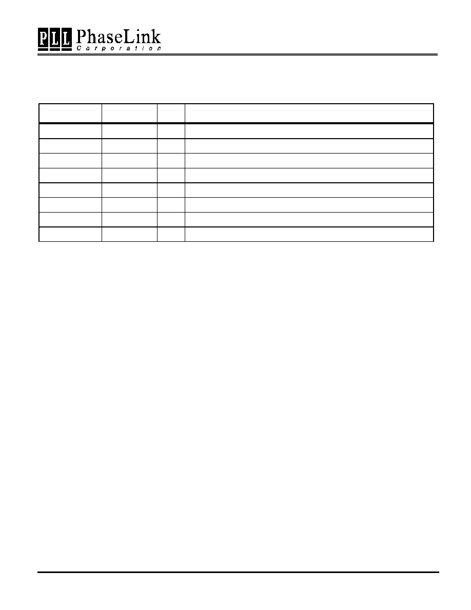
PIN DESCRIPTIONS
Name
Number
Type
Description
XIN
1
I
Crystal input connection (parallel mode crystal, C
L
= 14pF).
VDD
2
P
3.3V Power Supply.
VIN
3
I
Voltage Input for VCXO Frequency Control.
GND
4
P
Ground for PLL Core.
CLK
5
O
Clock Output.
VDD
6
P
3.3V Power Supply.
GND
7
P
Ground.
XOUT
8
O
Crystal connection.

PLL501-21/23
VCXO Clock Generator IC
47745 Fremont Blvd., Fremont, California 94538 TEL (510) 492-0990 FAX (510) 492-0991 Rev 01/15/01 Page 3
ELECTRICAL SPECIFICATIONS
1. Absolute Maximum Ratings
PARAMETERS
SYMBOL
MIN.
MAX.
UNITS
Supply Voltage
V
DD
7
V
Input Voltage, dc
V
I
V
SS
-
0.5
V
DD
+
0.5
V
Output Voltage, dc
V
O
V
SS
-
0.5
V
DD
+
0.5
V
Storage Temperature
T
S
-65
150
∞
C
Ambient Operating Temperature
T
A
0
70
∞
C
Junction Temperature
T
J
125
∞
C
Lead Temperature (soldering, 10s)
260
∞
C
Input Static Discharge Voltage Protection
2
KV
Exposure of the device under conditions beyond the limits specified by Maximum Ratings for extended periods may cause permanent damage to the
device and affect product reliability. These conditions represent a stress rating only, and functional operations of the device at these or any other
conditions above the operational limits noted in this specification is not implied.
2. DC Electrical Specifications
PARAMETERS
SYMBOL
CONDITIONS
MIN.
TYP.
MAX.
UNITS
Supply Current, Dynamic,
with Loaded Outputs
I
DD
f
XTA
= 13.5MHz
Ouput load of 4pF
20
mA
Operating Voltage
V
DD
3.13
3.47
V
Output High Voltage
V
OH
I
OH
= -12mA
2.4
V
Output Low Voltage
V
OL
I
LO
= 12mA
0.4
V
Output High Voltage at
CMOS level
V
OHC
I
OH
= -4mA
V
DD
≠ 0.4
V
Operating Supply Current
I
DD
No Load
7
mA
Short Circuit Current
±
50
mA
VIN, VCXO Control Voltage
0
3.3
V

PLL501-21/23
VCXO Clock Generator IC
47745 Fremont Blvd., Fremont, California 94538 TEL (510) 492-0990 FAX (510) 492-0991 Rev 01/15/01 Page 4
3. AC Electrical Specifications
PARAMETERS
SYMBOL
CONDITIONS
MIN.
TYP.
MAX.
UNITS
Input Crystal Frequency
13.5
MHz
Input Crystal Accuracy
±
30
ppm
Output Clock Rise Time
t
r
0.8V ~ 2.0V
1.5
ns
Output Clock Fall Time
t
f
2.0V ~ 0.8V
1.5
ns
Output Clock Duty Cycle
Measured @ 1.4V
45
50
55
%
Max Absolute Jitter
Short Term
100
ps
Short Circuit Current
±
50
mA
CLK output pullability
0V
VIN
3.3V
±
100
ppm
4. Voltage Control Crystal Oscillator
PARAMETERS
SYMBOL
CONDITIONS
MIN.
TYP.
MAX.
UNITS
PLL Stabilization Time *
T
PLLSTB
From VCXO stable
500
us
VCXO Stabilization Time *
T
VCXOSTB
From power valid
10
ms
Output Frequency Synthesis
Error
(Unless otherwise noted in
Frequency Table)
±
30
ppm
Crystal Resonator
Frequency
f
XTAL
Parallel Fundamental
Mode
10
13.5
15
MHz
Crystal Loading
Capacitance
C
L(xtal)
V
XTUNE
=1.65V
14
pF
Crystal Resonator Motional
Capacitance
C
1(xtal)
At cut
25
fF
VCXO Tuning Range
f
XTA
= 13.5MHz;
C
L
=14pF; C
MOT
=25fF
200
ppm
VCXO Tuning Characteristic
100
ppm/V
Note: Parameters denoted with an asterisk ( * ) represent nominal characterization data and are not production tested to any specific limits.
External Components
The PLL501-21/23 requires a minimum number of external components for proper operation. A
decoupling capacitor of 0.01
µ
F should be connected between VDD and GND on pin2 and 4, as close to
the PLL501-21/23 as possible. A series termination resistor of 33
may be used for the clock output.
The input crystal must be connected as close to the chip as possible. The input crystal should be a
parallel mode, pullable, AT cut, 13.5MHz, with 14pF load capacitance and a C0/C1 ratio of maximum
250. Consult PhaseLink for recommended suppliers.

PLL501-21/23
VCXO Clock Generator IC
47745 Fremont Blvd., Fremont, California 94538 TEL (510) 492-0990 FAX (510) 492-0991 Rev 01/15/01 Page 5
PACKAGE INFORMATION
ORDERING INFORMATION
PhaseLink Corporation, reserves the right to make changes in its products or specifications, or both at any time without notice. The information
furnished by Phaselink is believed to be accurate and reliable. However, PhaseLink makes no guarantee or warranty concerning the accuracy of said
information and shall not be responsible for any loss or damage of whatever nature resulting from the use of, or reliance upon this product.
LIFE SUPPORT POLICY: PhaseLink's products are not authorized for use as critical components in life support devices or systems without the
express written approval of the President of PhaseLink Corporation.
For part ordering, please contact our Sales Department:
47745 Fremont Blvd., Fremont, CA 94538, USA
Tel: (510) 492-0990 Fax: (510) 492-0991
PART NUMBER
The order number for this device is a combination of the following:
Device number, Package type and Operating temperature range
PLL501-21 S C
PART NUMBER
TEMPERATURATRE
C=COMMERCIAL
M=MILITARY
I=INDUSTRAL
PACKAGE TYPE
S=SOIC
C
L
A
8 PIN Narrow SOIC ( mm )
SOIC
Symbol
Min.
Max.
A
1.55
1.73
A1
0.15
0.18
B
0.35
0.49
C
0.19
0.25
D
4.80
4.98
E
3.81
3.99
H
5.84
6.20
L
0.41
0.89
e
1.27 BSC
E
H
D
A
1
e
B