Preliminary for proposal
PLL502-01
Low Phase Noise VCXO (24MHz to 50MHz)
47745 Fremont Blvd., Fremont, California 94538 TEL (510) 492-0990 FAX (510) 492-0991 Rev 4/01/02 Page 1
FEATURES
∑
Low phase noise VCXO output for the 24MHz to
50MHz range (-130 dBc at 10kHz offset).
∑
CMOS output.
∑
12 to 25MHz crystal input.
∑
Integrated variable capacitors.
∑
Selectable High Drive (36mA drive capability at
TTL level) or Standard Drive (12mA drive capa-
bility at TTL) output.
∑
Wide pull range (+/- 250 ppm).
∑
Low jitter (RMS): 10ps period.
∑
3.3V operation.
∑
Available in 8-Pin TSSOP or SOIC.
DESCRIPTIONS
The PLL502-01 is a low cost, high performance and
low phase noise VCXO, providing less than -130dBc
at 10kHz offset in the 24MHz to 50MHz operating
range. The very low jitter (10 ps RMS period jitter)
makes this chip ideal for applications requiring volt-
age controlled frequency sources. Input crystal can
range from 12 to 25MHz (fundamental resonant
mode).
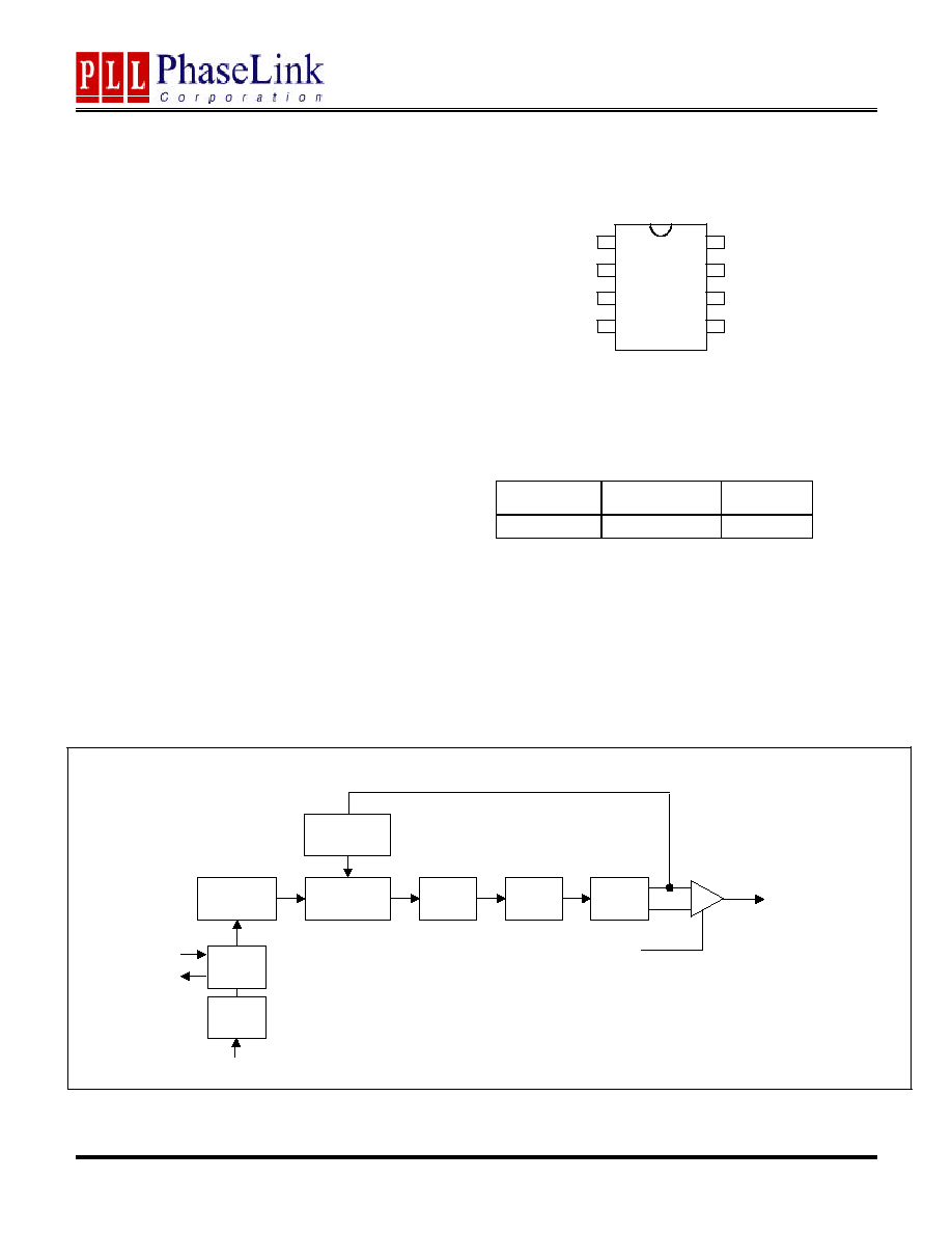
PIN CONFIGURATION
OUTPUT RANGE
MULTIPLIER
FREQUENCY
RANGE
OUTPUT
BUFFER
x2
24 - 50MHz
CMOS
BLOCK DIAGRAM
Reference
Divider
Phase
Comparator
Charge
Pump
Loop
Filter
VCO
VCO
Divider
XTAL
OSC
OE
XIN
XOUT
CLK
VIN
VARICAP
PLL502-01
1
2
3
4
5
6
7
8
XOUT
N/C
VIN
GND
XIN
VDD
CLK
OE
Preliminary for proposal
PLL502-01
Low Phase Noise VCXO (24MHz to 50MHz)
47745 Fremont Blvd., Fremont, California 94538 TEL (510) 492-0990 FAX (510) 492-0991 Rev 4/01/02 Page 2
PIN DESCRIPTIONS
Name
Number
Type
Description
XOUT
1
I
Crystal output pin.
N/C
2
-
Not connected.
VIN
3
I
Frequency control voltage input pin.
GND
4
P
Ground pin.
CLK
5
O
Output clock pin.
VDD
6
P
+3.3V VDD power supply pin.
OE
7
I
Output enable input pin. Disables (tri-state) output when low. Internal pull-
up enables output by default if pin is not connected to low.
XIN
8
I
Crystal input pin.
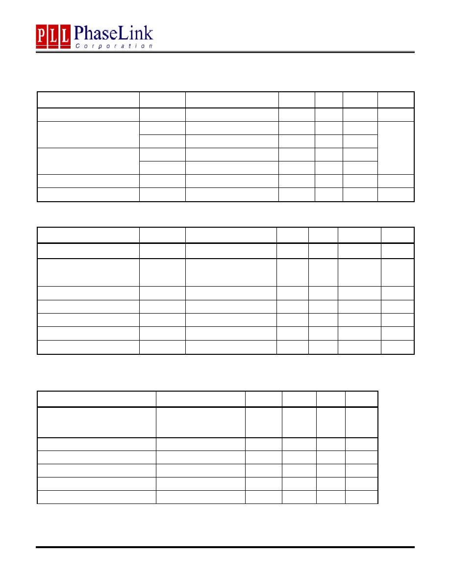
ELECTRICAL SPECIFICATIONS
1. Absolute Maximum Ratings
PARAMETERS
SYMBOL
MIN.
MAX.
UNITS
Supply Voltage Range
V
CC
-
0.5
7
V
Input Voltage Range
V
I
-
0.5
V
CC
+
0.5
V
Output Voltage Range
V
O
-
0.5
V
CC
+
0.5
V
Soldering Temperature
260
∞
C
Storage Temperature
T
S
-65
150
∞
C
Ambient Operating Temperature*
-40
85
∞
C
Exposure of the device under conditions beyond the limits specified by Maximum Ratings for extended periods may cause permanent damage to the
device and affect product reliability. These conditions represent a stress rating only, and functional operations of the device at these or any other
conditions above the operational limits noted in this specification is not implied.
* Note: Operating Temperature is guaranteed by design for all parts (COMMERCIAL and INDUSTRIAL), but tested for INDUSTRIAL grade only.
Preliminary for proposal
PLL502-01
Low Phase Noise VCXO (24MHz to 50MHz)
47745 Fremont Blvd., Fremont, California 94538 TEL (510) 492-0990 FAX (510) 492-0991 Rev 4/01/02 Page 3
2. AC Electrical Specifications
PARAMETERS
SYMBOL
CONDITIONS
MIN.
TYP.
MAX.
UNITS
Input Crystal Frequency
12
25
MHz
0.8V ~ 2.0V with 10 pF load
1.15
Output Clock Rise/Fall Time
(Low Drive)
0.3V ~ 3.0V with 15 pF load
3.7
0.8V ~ 2.0V with 10 pF load
0.5
Output Clock Rise/Fall Time
(High Drive)
0.3V ~ 3.0V with 15 pF load
1.5
ns
Output Clock Duty Cycle
Measured @ 1.4V
45
50
55
%
Short Circuit Current
±
50
mA
3. Voltage Control Crystal Oscillator
PARAMETERS
SYMBOL
CONDITIONS
MIN.
TYP.
MAX.
UNITS
VCXO Stabilization Time *
T
VCXOSTB
From power valid
10
ms
VCXO Tuning Range
F
XIN
= 12 ≠ 25MHz;
XTAL C
0
/C
1
< 250
500
ppm
CLK output pullability
0V
VIN
3.3V
±
250
ppm
VCXO Tuning Characteristic
165
ppm/V
Pull range linearity
10
%
VCON pin input impedance
2000
k
VCON modulation BW
0V
VIN
3.3V, -3dB
25
kHz
Note:
Parameters denoted with an asterisk (*) represent nominal characterization data and are not production tested to any specific limits.
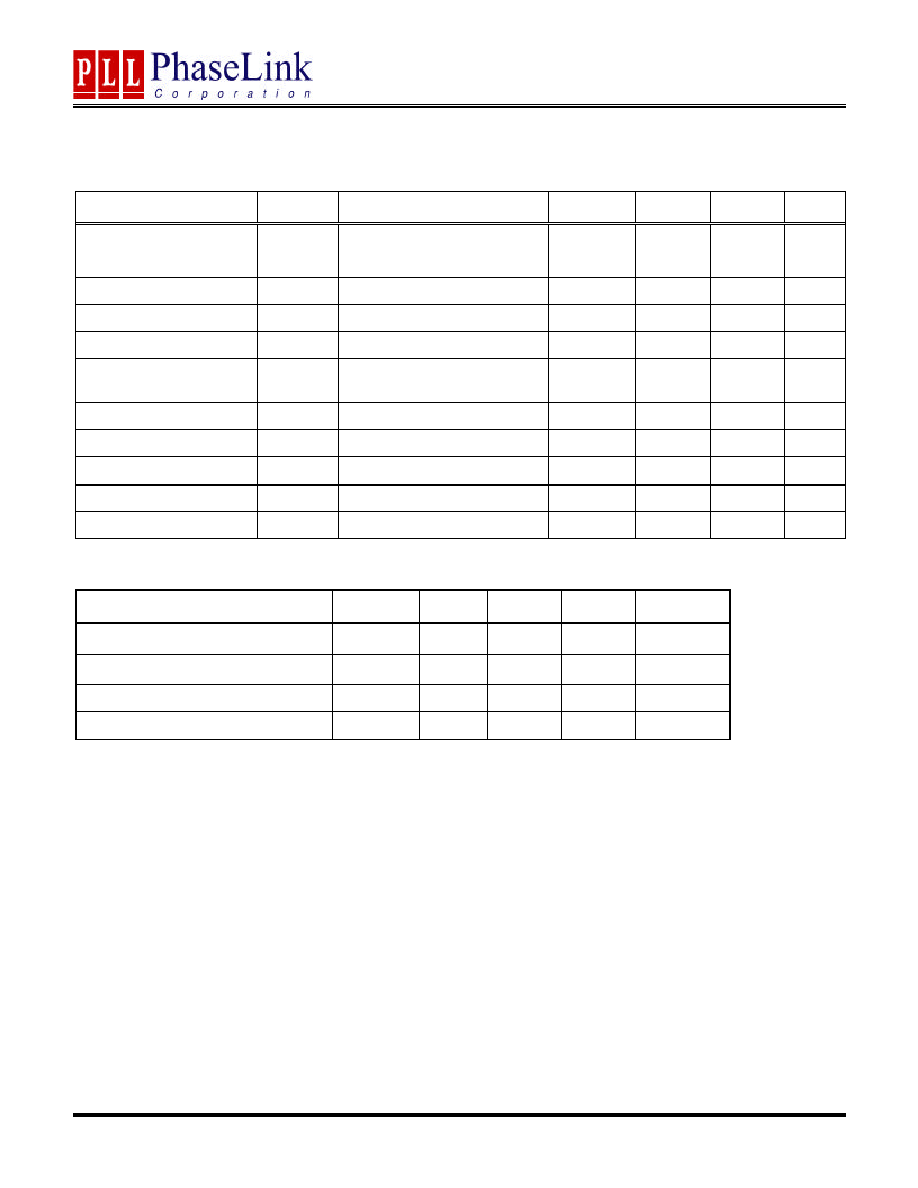
4. Jitter and Phase Noise specification
PARAMETERS
CONDITIONS
MIN.
TYP.
MAX. UNITS
RMS Period Jitter
(1 sigma ≠ 1000 samples)
at 44MHz, with capacitive
decoupling between VDD
and GND.
10
ps
Phase Noise relative to carrier
44MHz @100Hz offset
-80
dBc/Hz
Phase Noise relative to carrier
44MHz @1kHz offset
-110
dBc/Hz
Phase Noise relative to carrier
44MHz @10kHz offset
-130
dBc/Hz
Phase Noise relative to carrier
44MHz @100kHz offset
-123
dBc/Hz
Phase Noise relative to carrier
44MHz @1MHz offset
-124
dBc/Hz
Preliminary for proposal
PLL502-01
Low Phase Noise VCXO (24MHz to 50MHz)
47745 Fremont Blvd., Fremont, California 94538 TEL (510) 492-0990 FAX (510) 492-0991 Rev 4/01/02 Page 4
5. DC Specification
PARAMETERS
SYMBOL
CONDITIONS
MIN.
TYP.
MAX. UNITS
Supply Current, Dynamic,
with Loaded Outputs
I
DD
F
XIN
= 12 - 25MHz
Ouput load of 10pF
16
20
mA
Operating Voltage
V
DD
3.13
3.47
V
Output High Voltage
V
OH
I
OH
= -12mA (low drive)
2.4
V
Output Low Voltage
V
OL
I
LO
= 12mA (low drive)
0.4
V
Output High Voltage at
CMOS level
V
OHC
I
OH
= -4mA (low drive)
V
DD
≠ 0.4
V
Output drive current
At TTL level (High drive)
36
51
mA
At TTL level (Low drive)
12
17
mA
Short Circuit Current
±
50
mA
VCXO Control Voltage
VCON
0
3.3
V
ESD Protection
Human Body Model
3000
6. Crystal Specifications
PARAMETERS
SYMBOL
MIN.
TYP.
MAX.
UNITS
Crystal Resonator Frequency
F
XIN
12
25
MHz
Crystal Loading Capacitance Rating
C
L
(xtal)
9.5
pF
C0/C1
250
-
ESR
R
S
30
Note
: Crystal Loading rating: 9.5pF is the loading the crystal sees from the VCXO chip at VCON = 1.65V. It is assumed that the crystal will be at
nominal frequency at this load. If the crystal requires more load to be at nominal frequency, the additional load must be added externally.
This however may reduce the pull range.
Preliminary for proposal
PLL502-01
Low Phase Noise VCXO (24MHz to 50MHz)
47745 Fremont Blvd., Fremont, California 94538 TEL (510) 492-0990 FAX (510) 492-0991 Rev 4/01/02 Page 5
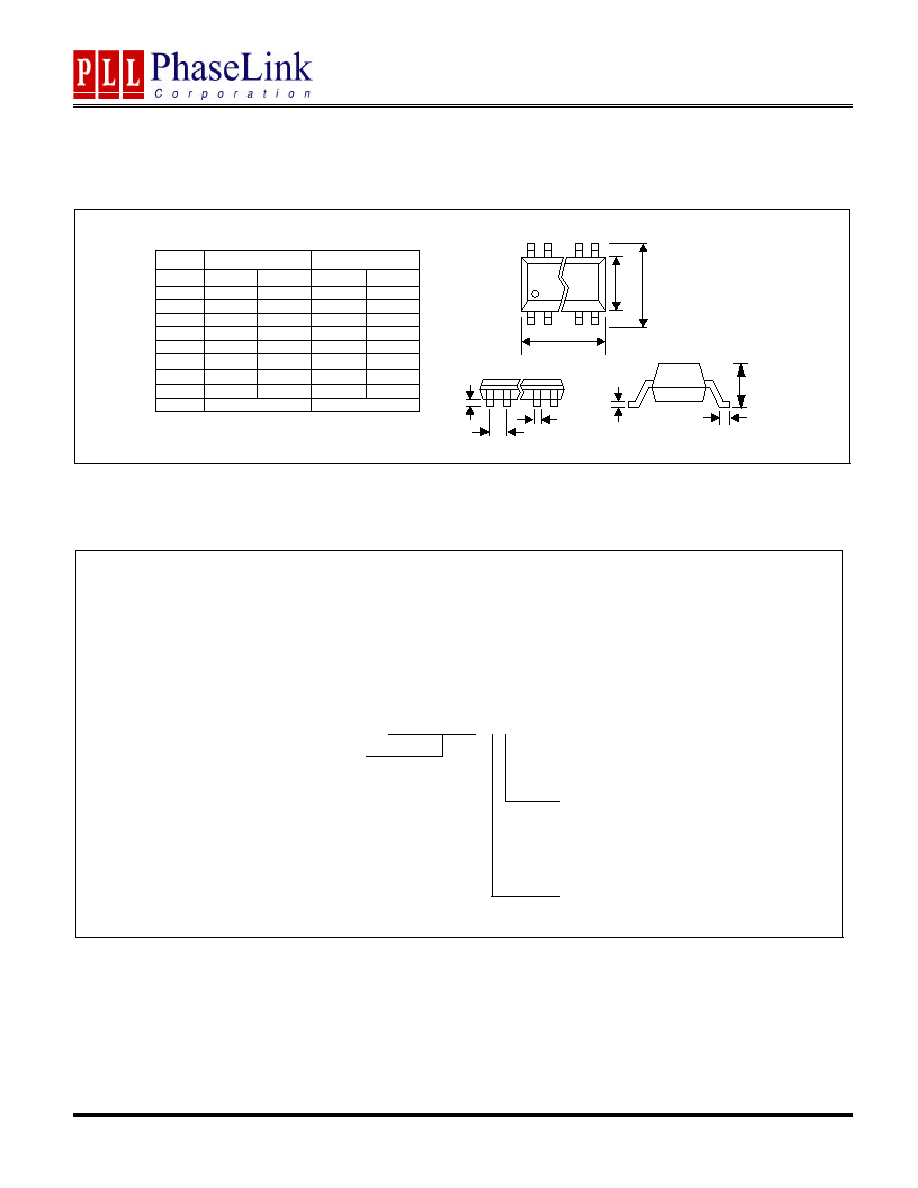
PACKAGE INFORMATION
ORDERING INFORMATION
PhaseLink Corporation, reserves the right to make changes in its products or specifications, or both at any time without notice. The information fur-
nished by Phaselink is believed to be accurate and reliable. However, PhaseLink makes no guarantee or warranty concerning the accuracy of said
information and shall not be responsible for any loss or damage of whatever nature resulting from the use of, or reliance upon this product.
LIFE SUPPORT POLICY
: PhaseLink's products are not authorized for use as critical components in life support devices or systems without the ex-
press written approval of the President of PhaseLink Corporation.
For part ordering, please contact our Sales Department:
47745 Fremont Blvd., Fremont, CA 94538, USA
Tel: (510) 492-0990 Fax: (510) 492-0991
PART NUMBER
The order number for this device is a combination of the following:
Device number, Package type and Operating temperature range
PLL502-01 X C
PART NUMBER
TEMPERATURATURE
C=COMMERCIAL
M=MILITARY
I=INDUSTRAL
PACKAGE TYPE
S=SOIC, O=TSSOP
C
L
A
8 PIN ( dimensions in mm )
Narrow SOIC
Symbol
Min.
Max.
A
1.47
1.73
A1
0.10
0.25
B
0.33
0.51
C
0.19
0.25
D
4.80
4.95
E
3.80
4.00
H
5.80
6.20
L
0.38
1.27
e
1.27 BSC
E
H
D
A1
e
B
TSSOP
Min.
Max.
-
1.20
0.05
0.15
0.19
0.30
0.09
0.20
2.90
3.10
4.30
4.50
6.20
6.60
0.45
0.75
0.65 BSC