Preliminary
PLL502-14
192MHz ≠ 400MHz Low Phase Noise LVDS VCXO (12 ≠ 25MHz Crystal)
47745 Fremont Blvd., Fremont, California 94538 TEL (510) 492-0990 FAX (510) 492-0991 Rev 7/15/02 Page 1
FEATURES
∑
Low phase noise output for the 192MHz to
400MHz range (-132 dBc at 10kHz offset).
∑
LVDS output.
∑
12 to 25MHz crystal input.
∑
Integrated crystal load capacitor: no external
load capacitor required.
∑
Output Enable selector.
∑
Wide pull range (min. +/-190 ppm)
∑
3.3V operation.
∑
Available in 16 Pin TSSOP or SOIC.
DESCRIPTION
The PLL502-14 is a monolithic low jitter and low
phase noise (-115dBc/Hz @ 10kHz offset) VCXO IC
with LVDS output, for 192MHz to 400MHz output
range. It allows the control of the output frequency
with an input voltage (VIN), using a low cost crystal.
The chip provides a pullable output at a frequency of
F
XIN
x 16. This makes the PLL502-14 ideal for a wide
range of applications.
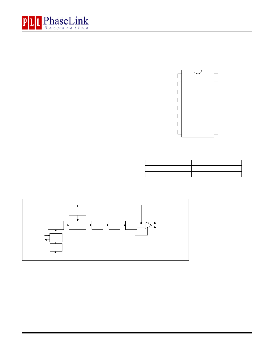
PIN CONFIGURATION
F
OUT
= F
XIN
x 16
OE (Pin 5)
Output State
0
Tri-state
1 (Default)
Output enabled
BLOCK DIAGRAM
Reference
Divider
Phase
Comparator
Charge
Pump
Loop
Filter
VCO
VCO
Divider
XTAL
OSC
CLKBAR
OE
XIN
XOUT
CLK
VIN
VARICAP
PLL 502-14
1
2
3
4
5
6
7
8
VDD
9
10
11
12
13
14
15
16
VDD
XIN
XOUT
OE
VIN
GND
GND
VDD
GND_BUF
CLKBAR
VDD_BUF
CLK
GND_BUF
GND
GND
Preliminary
PLL502-14
192MHz ≠ 400MHz Low Phase Noise LVDS VCXO (12 ≠ 25MHz Crystal)
47745 Fremont Blvd., Fremont, California 94538 TEL (510) 492-0990 FAX (510) 492-0991 Rev 7/15/02 Page 2
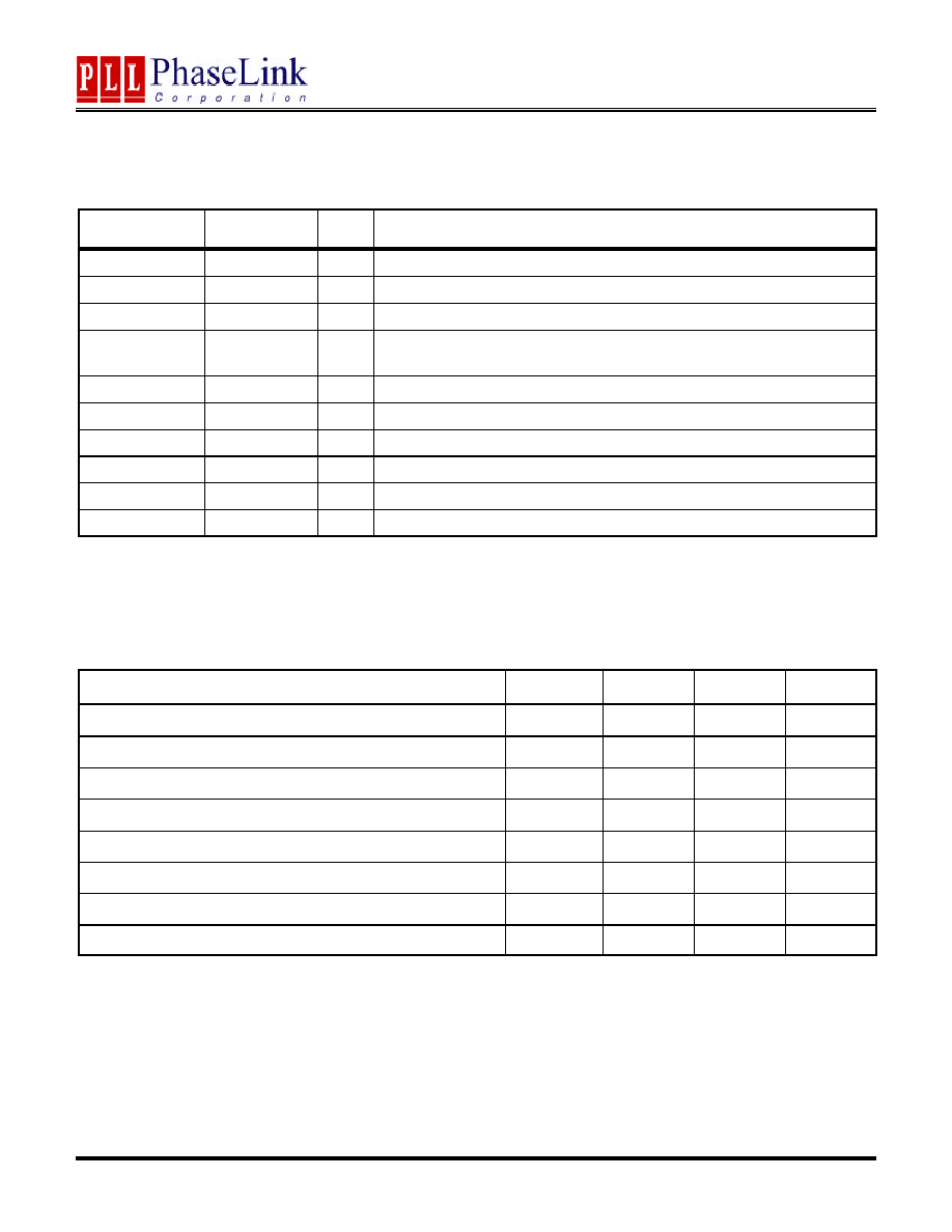
PIN DESCRIPTIONS
Name
Number
Type
Description
VDD
1,2,16
P
+3.3V Power supply connectors.
XIN
3
I
Crystal input pin.
XOUT
4
I
Crystal output pin.
OE
5
I
Output enable input pin. Disables (tri-state) output when low. Internal
pull-up enables output by default if pin is not connected to low.
VIN
6
I
Frequency control voltage input pin.
GND
7,8,9,10
P
GND Power connectors.
GND_BUF
11,15
P
GND connector for output buffers.
CLK
12
O
True clock output pin.
VDD_BUF
13
P
+3.3V Power supply connector for output buffers.
CLKB
14
O
Complementary clock output pin.
ELECTRICAL SPECIFICATIONS
1. Absolute Maximum Ratings
PARAMETERS
SYMBOL
MIN.
MAX.
UNITS
Supply Voltage
V
DD
7
V
Input Voltage, dc
V
I
V
SS
-
0.5
V
DD
+
0.5
V
Output Voltage, dc
V
O
V
SS
-
0.5
V
DD
+
0.5
V
Storage Temperature
T
S
-65
150
∞
C
Ambient Operating Temperature*
T
A
-40
85
∞
C
Junction Temperature
T
J
125
∞
C
Lead Temperature (soldering, 10s)
260
∞
C
Input Static Discharge Voltage Protection
2
kV
Exposure of the device under conditions beyond the limits specified by Maximum Ratings for extended periods may cause permanent damage to the
device and affect product reliability. These conditions represent a stress rating only, and functional operations of the device at these or any other
conditions above the operational limits noted in this specification is not implied.
Preliminary
PLL502-14
192MHz ≠ 400MHz Low Phase Noise LVDS VCXO (12 ≠ 25MHz Crystal)
47745 Fremont Blvd., Fremont, California 94538 TEL (510) 492-0990 FAX (510) 492-0991 Rev 7/15/02 Page 3
2. Crystal Specifications
PARAMETERS
SYMBOL
CONDITIONS
MIN.
TYP.
MAX.
UNITS
Crystal Resonator
Frequency
F
XIN
Parallel Fundamental
Mode
12
25
MHz
Crystal Loading Rating
C
L
(xtal)
At VIN = 1.65V
9.5
pF
Crystal Pullability
C
0
/C
1
(xtal)
AT cut
250
-
Recommended ESR
R
E
AT cut
30
Note
: Crystal Loading rating: 9.5pF is the loading the crystal sees from the VCXO chip at VIN = 1.65V. It is assumed that the crystal will be at nominal
frequency at this load. If the crystal requires more load to be at nominal frequency, the additional load must be added externally. This however may
reduce the pull range.
3. Voltage Control Crystal Oscillator
PARAMETERS
SYMBOL
CONDITIONS
MIN.
TYP.
MAX.
UNITS
VCXO Stabilization Time *
T
VCXOSTB
From power valid
10
ms
VCXO Tuning Range
F
XIN
= 12 - 25MHz;
XTAL C
0
/C
1
< 250
380
ppm
CLK output pullability
0V
VCON
3.3V
±
190
ppm
Linearity
5
10
%
VCXO Tuning Characteristic
115
ppm/V
VCON pin input impedance
2000
k
VCON modulation BW
0V
VCON
3.3V, -3dB
25
kHz
Note:
Parameters denoted with an asterisk (*) represent nominal characterization data and are not production tested to any specific limits.
4. General Electrical Specifications
PARAMETERS
SYMBOL
CONDITIONS
MIN.
TYP.
MAX.
UNITS
Supply Current, Dynamic
(with Loaded Outputs)
I
DD
LVDS
60
mA
Operating Voltage
V
DD
3.13
3.47
V
Output Clock Duty Cycle
@ 1.25V (LVDS)
45
50
55
%
Short Circuit Current
±
50
mA
Preliminary
PLL502-14
192MHz ≠ 400MHz Low Phase Noise LVDS VCXO (12 ≠ 25MHz Crystal)
47745 Fremont Blvd., Fremont, California 94538 TEL (510) 492-0990 FAX (510) 492-0991 Rev 7/15/02 Page 4
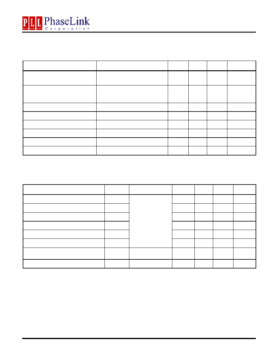
5. Jitter and Phase Noise specification
PARAMETERS
CONDITIONS
MIN.
TYP.
MAX.
UNITS
Period jitter RMS at 311MHz
With capacitive decoupling
between VDD and GND.
9
ps
Accumulated jitter RMS at
311MHz
With capacitive decoupling
between VDD and GND. Over
10,000 cycles.
TBM
ps
Integrated jitter RMS at 311MHz
Integrated 12 kHz to 20 MHz
4
ps
Phase Noise relative to carrier
311MHz @10Hz offset
-60
dBc/Hz
Phase Noise relative to carrier
311MHz @100Hz offset
-90
dBc/Hz
Phase Noise relative to carrier
311MHz @1kHz offset
-111
dBc/Hz
Phase Noise relative to carrier
311MHz @10kHz offset
-115
dBc/Hz
Phase Noise relative to carrier
311MHz @100kHz offset
-110
dBc/Hz
Note: Phase Noise measured at VIN = 0V
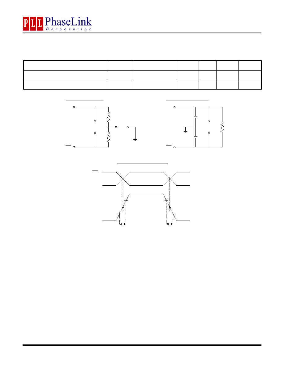
6. LVDS Electrical Characteristics
PARAMETERS
SYMBOL
CONDITIONS
MIN.
TYP.
MAX.
UNITS
Output Differential Voltage
V
OD
247
355
454
mV
V
DD
Magnitude Change
V
OD
-50
50
mV
Output High Voltage
V
OH
1.4
1.6
V
Output Low Voltage
V
OL
0.9
1.1
V
Offset Voltage
V
OS
1.125
1.2
1.375
V
Offset Magnitude Change
V
OS
R
L
= 100
(see figure)
0
3
25
mV
Power-off Leakage
I
OXD
V
out
= V
DD
or GND
V
DD
= 0V
±
1
±
10
uA
Output Short Circuit Current
I
OSD
-5.7
-8
mA
Preliminary
PLL502-14
192MHz ≠ 400MHz Low Phase Noise LVDS VCXO (12 ≠ 25MHz Crystal)
47745 Fremont Blvd., Fremont, California 94538 TEL (510) 492-0990 FAX (510) 492-0991 Rev 7/15/02 Page 5
7. LVDS Switching Characteristics
PARAMETERS
SYMBOL
CONDITIONS
MIN.
TYP.
MAX.
UNITS
Differential Clock Rise Time
t
r
0.2
0.7
1.0
ns
Differential Clock Fall Time
t
f
R
L
= 100
C
L
= 10 pF
(see figure)
0.2
0.7
1.0
ns
OUT
OUT
V
OD
V
OS
50
50
OUT
V
DIFF
R
L
= 100
C
L
= 10pF
C
L
= 10pF
LVDS Switching Test Circuit
LVDS Levels Test Circuit
LVDS Transistion Time Waveform
OUT
OUT
OUT
0V (Differential)
0V
20%
80%
20%
80%
t
R
t
F
V
DIFF
Preliminary
PLL502-14
192MHz ≠ 400MHz Low Phase Noise LVDS VCXO (12 ≠ 25MHz Crystal)
47745 Fremont Blvd., Fremont, California 94538 TEL (510) 492-0990 FAX (510) 492-0991 Rev 7/15/02 Page 6
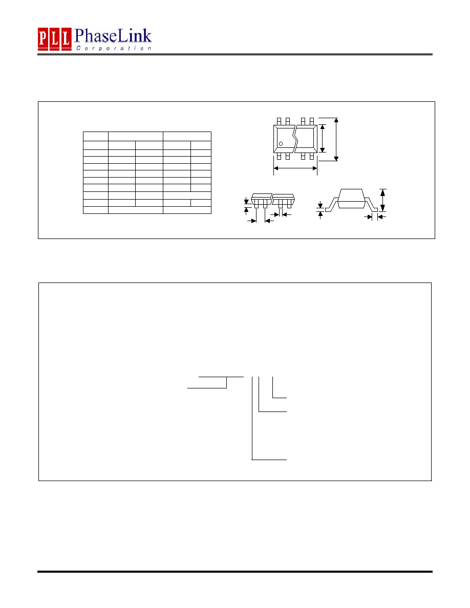
PACKAGE INFORMATION
ORDERING INFORMATION
PhaseLink Corporation, reserves the right to make changes in its products or specifications, or both at any time without notice. The information
furnished by Phaselink is believed to be accurate and reliable. However, PhaseLink makes no guarantee or warranty concerning the accuracy of said
information and shall not be responsible for any loss or damage of whatever nature resulting from the use of, or reliance upon this product.
LIFE SUPPORT POLICY
: PhaseLink's products are not authorized for use as critical components in life support devices or systems without the
express written approval of the President of PhaseLink Corporation.
For part ordering, please contact our Sales Department:
47745 Fremont Blvd., Fremont, CA 94538, USA
Tel: (510) 492-0990 Fax: (510) 492-0991
PART NUMBER
The order number for this device is a combination of the following:
Device number, Package type and Operating temperature range
PLL502-14 S C XX
PART NUMBER
TEMPERATURATURE
C=COMMERCIAL
M=MILITARY
I=INDUSTRAL
PACKAGE TYPE
S=SOIC, O=TSSOP
REVISION CODE
(when applicable)
C
L
A
16 PIN Narrow SOIC, TSSOP ( mm )
SOIC
TSSOP
Symbol
Min.
Max.
Min.
Max.
A
1.35
1.75
-
1.20
A1
0.10
0.25
0.05
0.15
B
0.33
0.51
0.19
0.30
C
0.19
0.25
0.09
0.20
D
9.80
10.00
4.90
5.10
E
3.80
4.00
4.30
4.50
H
5.80
6.20
6.40 BSC
L
0.40
1.27
0.45
0.75
e
1.27 BSC
0.65 BSC
E
H
D
A1
e
B