 | –≠–ª–µ–∫—Ç—Ä–æ–Ω–Ω—ã–π –∫–æ–º–ø–æ–Ω–µ–Ω—Ç: PLL520-08 | –°–∫–∞—á–∞—Ç—å:  PDF PDF  ZIP ZIP |
PLL520-05/-06/-07/-08/-09
Low Phase Noise VCXO with multipliers (for 100-200MHz Fund Xtal)
47745 Fremont Blvd., Fremont, California 94538 Tel (510) 492-0990 Fax (510) 492-0991 www.phaselink.com Rev 09/20/04 Page 1
FEATURES
∑ 100MHz to 200MHz Fundamental Mode Crystal.
∑ Output range: 100 ≠ 200MHz (no multiplication),
200 ≠ 400MHz (2x multiplier), 400 ≠ 800MHz (4x
multiplier), or 800MHz ≠ 1GHz (PLL520-09
TSSOP only, 8x multiplier).
∑ High yield design supports up to 2pF stray
capacitance at 200MHz.
∑ CMOS (Standard drive PLL520-07 or Selectable
Drive PLL520-06), PECL (Enable low PLL520-08
or Enable high PLL520-05) or LVDS output
(PLL520-09).
∑ Integrated variable capacitors.
∑ Supports 3.3V-Power Supply.
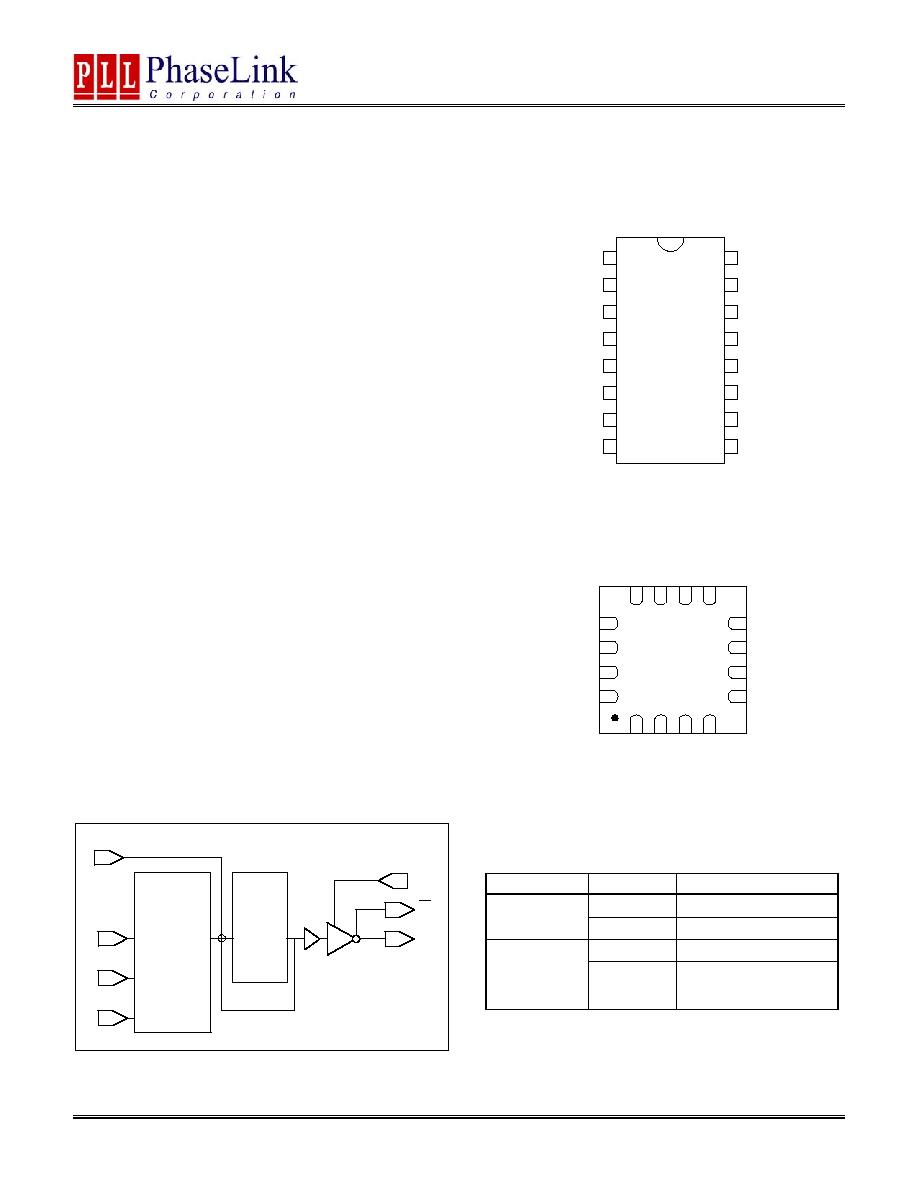
∑ Available in 16-Pin (TSSOP or 3x3mm QFN)
Note: PLL520-06 only available in 3x3mm.
Note: PLL520-07 only available in TSSOP.
DESCRIPTION
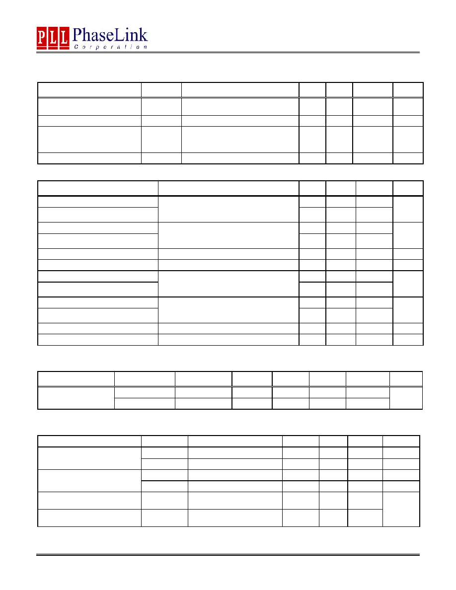
The PLL520-05/-06/-07/-08/-09 is a family of VCXO
ICs specifically designed to pull high frequency
fundamental crystals. Their design was optimized to
tolerate higher limits of interelectrode capacitance
and bonding capacitance to improve yield. They
achieve very low current into the crystal resulting in
better overall stability. Their internal varicaps allow
an on chip frequency pulling, controlled by the
VCON input.
BLOCK DIAGRAM
PIN CONFIGURATION
(Top View)
^: Internal pull-up
*: PLL520-06 pin 12 is output drive select (DRIVSEL)
(0 for High Drive CMOS, 1 for Standard Drive CMOS)
OUTPUT ENABLE LOGICAL LEVELS
Part #
OE
State
0 (Default) Output enabled
PLL520-08
1 Tri-state
0 Tri-state
PLL520-05
PLL520-06
PLL520-07
PLL520-09
1 (Default) Output enabled
OE input: Logical states defined by PECL levels for PLL520-08
Logical states defined by CMOS levels for PLL520-05/-06/-
07/-09
XIN
XOUT
OE
Q
VCON
Q
PLL by-pass
SEL
PLL
(Phase
Locked
Loop)
Oscillator
Amplifier
w/
integrated
varicaps
PLL 520-0x
1
2
3
4
5
6
7
8
VDD
9
10
11
12
13
14
15
16
XIN
XOUT
SEL3^
SEL2^
OE
VCON
GND
SEL0^
SEL1^
GND
CLKC
VDD
CLKT
GND
GND
P520-0x
GND
VDD
CLKT
CLKC
G
N
D
/
DR
IVSE
L*
SEL
0^
SEL
1^
VD
D
XOUT
XIN
SEL2^
OE
GND
VC
ON
GND
GND
4
16
15
14
13
12
11
10
9
8
7
6
5
1
2
3
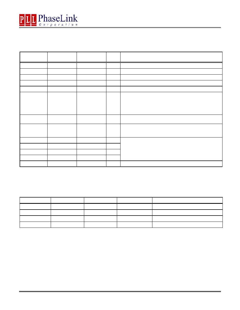
PLL520-05/-06/-07/-08/-09
Low Phase Noise VCXO with multipliers (for 100-200MHz Fund Xtal)
47745 Fremont Blvd., Fremont, California 94538 Tel (510) 492-0990 Fax (510) 492-0991 www.phaselink.com Rev 09/20/04 Page 2
PIN DESCRIPTIONS
Name
TSSOP*
Pin number
3x3mm QFN*
Pin number
Type Description
XIN
2
13
I
Crystal in connector.
XOUT 3 14
I
Crystal
out
connector.
OE 6 16
I
Output
enable
pin.
VCON
7
1
I
Frequency control input (0.3V to 3.0V)
GND
8,9, 10, 14
2,3,4,8,12
P
Ground (except pin 12 on PLL520-06: DRIVSEL see below).
DRIVSEL** -
12 I
PLL520-06 only: Drive Select Input. This pin has an internal
pull-up that will default DRIVSEL to `1' when not connect to
GND. CMOS output of PLL520-06 will be high drive CMOS
when DRIVSEL is set to `0', and will be standard CMOS
otherwise.
CLKT 11
5
O
True output PECL (PLL520-08) or LVDS (PLL520-09)
(N/C for PLL520-07)
CLKC 13
7 O
Complementary output PECL (PLL520-08) or LVDS
(PLL520-09)
(CMOS out for PLL520-07).
SEL0 16 10
I
SEL1 15 9 I
SEL2 5 15
I
SEL3 4
Not
available
I
Multiplier selector pins. These pins have an internal pull-up
that will default SEL to `1' when not connected to GND.
VDD
1, 12
6,11
P
+3.3V power supply.
* Note: PLL520-06 only available in 3x3mm QFN, PLL520-07 only available in TSSOP.
** Note: DRIVSEL on pin 12 on PLL520-06 only.
FREQUENCY SELECTION TABLE
SEL3* SEL2 SEL1 SEL0
Selected
Multiplier
0*
0
1
1
Fin x 8 (PLL520-09 in TSSOP only)
1*
0
1
1
Fin x 4
1*
1
1
0
Fin x 2
1* 1 1 1
No
multiplication
Note *: SEL3 is not available (always "1") in 3x3mm package
All pins have internal pull-ups (default value is 1). Connect to GND to set to 0.

PLL520-05/-06/-07/-08/-09
Low Phase Noise VCXO with multipliers (for 100-200MHz Fund Xtal)
47745 Fremont Blvd., Fremont, California 94538 Tel (510) 492-0990 Fax (510) 492-0991 www.phaselink.com Rev 09/20/04 Page 3
ELECTRICAL SPECIFICATIONS
1. Absolute Maximum Ratings
PARAMETERS SYMBOL
MIN.
MAX.
UNITS
Supply Voltage
V
DD
4.6 V
Input Voltage, dc
V
I
-0.5
V
DD
+0.5 V
Output Voltage, dc
V
O
-0.5
V
DD
+0.5 V
Storage Temperature
T
S
-65 150
∞C
Ambient Operating Temperature*
T
A
-40 85
∞C
Junction Temperature
T
J
125
∞C
Lead Temperature (soldering, 10s)
260
∞C
ESD Protection, Human Body Model
2
kV
Exposure of the device under conditions beyond the limits specified by Maximum Ratings for extended periods may cause permanent damage to the
device and affect product reliability. These conditions represent a stress rating only, and functional operations of the device at these or any other
conditions above the operational limits noted in this specification is not implied.
* Note: Operating Temperature is guaranteed by design for all parts (COMMERCIAL and INDUSTRIAL), but tested for COMMERCIAL grade only.
2. Crystal Specifications
3. Voltage Controlled Crystal Oscillator
PARAMETERS SYMBOL CONDITIONS MIN.
TYP.
MAX.
UNITS
VCXO Stabilization Time *
T
VCXOSTB
From power valid
10
ms
VCXO Tuning Range
F
XIN
= 100 ≠ 200MHz;
XTAL C
0
/C
1
< 250
0V
VCON 3.3V
200* ppm
CLK output pullability
VCON=1.65V,
±1.65V
±100*
ppm
On-chip Varicaps control range
VCON = 0 to 3.3V
4 ≠ 18*
pF
Linearity
10*
%
VCXO Tuning Characteristic
65
ppm/V
VCON input impedance
60
k
VCON modulation BW
0V
VCON 3.3V, -3dB
25 kHz
Note: Parameters denoted with an asterisk (*) represent nominal characterization data and are not production tested to any specific limits.
PARAMETERS SYMBOL CONDITIONS
MIN.
MAX.
UNITS
Crystal Resonator Frequency
F
XIN
Parallel Fundamental Mode
100
200
MHz
Crystal Loading Rating
C
L (xtal)
Die at VCON = 1.65V
4
pF
Interelectrode Capacitance
C
0
3.5
pF
Crystal Pullability
C
0
/C
1 (xtal)
AT
cut
250
-
Recommended ESR
R
E
AT cut
30
PLL520-05/-06/-07/-08/-09
Low Phase Noise VCXO with multipliers (for 100-200MHz Fund Xtal)
47745 Fremont Blvd., Fremont, California 94538 Tel (510) 492-0990 Fax (510) 492-0991 www.phaselink.com Rev 09/20/04 Page 4
4. General Electrical Specifications
PARAMETERS SYMBOL
CONDITIONS
MIN.
TYP.
MAX.
UNITS
Supply Current (Loaded
Outputs)
I
DD
PECL/LVDS/CMOS
100/80/40
mA
Operating Voltage
V
DD
2.97
3.63
V
Output Clock Duty Cycle
@ 50% V
DD
(CMOS)
@ 1.25V (LVDS)
@ V
DD
≠ 1.3V (PECL)
45
45
45
50
50
50
55
55
55
%
Short Circuit Current
±50
mA
5. Jitter Specifications
PARAMETERS CONDITIONS
MIN.
TYP.
MAX.
UNITS
Period jitter RMS
2.5
Period jitter peak-to-peak
At 155.52MHz, with capacitive decoupling
between VDD and GND. Over 10,000
cycles
18.5 20
ps
Accumulated jitter RMS
2.5
Accumulated jitter peak-to-peak
At 155.52MHz, with capacitive decoupling
between VDD and GND. Over 1,000,000
cycles.
24 27
ps
Random Jitter
"RJ" measured on Wavecrest SIA 3000
2.5
ps
Integrated jitter RMS at 155MHz
Integrated 12 kHz to 20 MHz
0.3
0.4
ps
Period jitter RMS
11
Period jitter peak-to-peak
At 622.08MHz, with capacitive decoupling
between VDD and GND. Over 10,000
cycles
45 49
ps
Accumulated jitter RMS
11
Accumulated jitter peak-to-peak
At 622.08MHz, with capacitive decoupling
between VDD and GND. Over 1,000,000
cycles.
24 27
ps
Random Jitter
"RJ" measured on Wavecrest SIA 3000
3
ps
Integrated jitter RMS at 622MHz
Integrated 12 kHz to 20 MHz
1.6
1.8
ps
Measured on Wavecrest SIA 3000
6. Phase Noise Specifications
PARAMETERS FREQUENCY @10Hz @100Hz @1kHz @10kHz @100kHz UNITS
155.52MHz -75 -95
-125
-140
-145
Phase Noise relative
to carrier
622.08MHz -75 -95
-110
-125
-120
dBc/Hz
Note: Phase Noise measured at VCON = 0V
7. CMOS Electrical Specifications
PARAMETERS SYMBOL CONDITIONS MIN.
TYP.
MAX.
UNITS
I
OH
V
OH
= V
DD
-0.4V, V
DD
=3.3V 30 mA
Output drive current
(High Drive)
I
OL
V
OL
= 0.4V, V
DD
= 3.3V
30
mA
I
OH
V
OH
= V
DD
-0.4V, V
DD
=3.3V 10 mA
Output drive current
(Standard Drive)
I
OL
V
OL
= 0.4V, V
DD
= 3.3V
10
mA
Output Clock Rise/Fall Time
(Standard Drive)
0.3V ~ 3.0V with 15 pF load
2.4
Output Clock Rise/Fall Time
(High Drive)
0.3V ~ 3.0V with 15 pF load
1.2
ns
* Note: High Drive CMOS is available on PLL520-06 through DRIVSEL selector input on pin 12.

PLL520-05/-06/-07/-08/-09
Low Phase Noise VCXO with multipliers (for 100-200MHz Fund Xtal)
47745 Fremont Blvd., Fremont, California 94538 Tel (510) 492-0990 Fax (510) 492-0991 www.phaselink.com Rev 09/20/04 Page 5
8. LVDS Electrical Characteristics
PARAMETERS SYMBOL
CONDITIONS
MIN.
TYP.
MAX.
UNITS
Output Differential Voltage
V
OD
247
355
454
mV
V
DD
Magnitude Change
V
OD
-50 50 mV
Output High Voltage
V
OH
1.4
1.6
V
Output Low Voltage
V
OL
0.9
1.1
V
Offset Voltage
V
OS
1.125
1.2
1.375
V
Offset Magnitude Change
V
OS
R
L
= 100
(see figure)
0 3 25 mV
Power-off Leakage
I
OXD
V
out
= V
DD
or GND
V
DD
= 0V
±1
±10
uA
Output Short Circuit Current
I
OSD
-5.7 -8
mA
9. LVDS Switching Characteristics
PARAMETERS SYMBOL
CONDITIONS
MIN.
TYP.
MAX.
UNITS
Differential Clock Rise Time
t
r
0.2 0.7 1.0 ns
Differential Clock Fall Time
t
f
R
L
= 100
C
L
= 10 pF
(see figure)
0.2 0.7 1.0 ns
OUT
OUT
V
OD
V
OS
50
50
OUT
V
DIFF
R
L
= 100
C
L
= 10pF
C
L
= 10pF
LVDS Switching Test Circuit
LVDS Levels Test Circuit
LVDS Transistion Time Waveform
OUT
OUT
OUT
0V (Differential)
0V
20%
80%
20%
80%
t
R
t
F
V
DIFF