 | –≠–ª–µ–∫—Ç—Ä–æ–Ω–Ω—ã–π –∫–æ–º–ø–æ–Ω–µ–Ω—Ç: PLL520-30 | –°–∫–∞—á–∞—Ç—å:  PDF PDF  ZIP ZIP |
Preliminary
PLL520-30
PECL and LVDS Low Phase Noise VCXO (for 65-130MHz Fund Xtal)
47745 Fremont Blvd., Fremont, California 94538 TEL (510) 492-0990 FAX (510) 492-0991 Rev 4/09/02 Page 1
FEATURES
∑
65MHz to 130MHz Fundamental Mode Crystal.
∑
Output range: 65MHz ≠ 130MHz (no PLL).
∑
Low Injection Power for crystal 50uW.
∑
Complementary outputs: PECL or LVDS.
∑
Integrated variable capacitors.
∑
Supports 3.3V-Power Supply.
∑
Available in die form.
∑
Thickness 10 mil.
DESCRIPTIONS
PLL520-30 is a VCXO IC specifically designed to
pull frequency fundamental crystals from 65MHz to
130MHz, with selectable PECL or LVDS outputs. Its
design was optimized to tolerate higher limits of
interelectrodes capacitance and bonding
capacitance to improve yield. It achieves very low
current into the crystal resulting in better overall
stability. Its internal varicaps allow an on chip
frequency pulling, controlled by the VCON input.
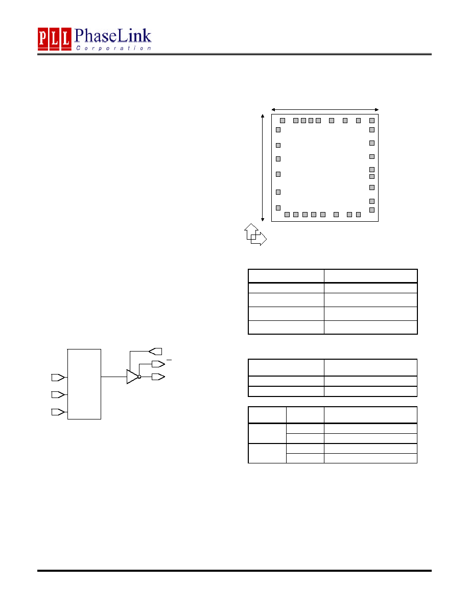
BLOCK DIAGRAM
DIE CONFIGURATION
DIE SPECIFICATIONS
Name
Value
Size
62 x 65 mil
Reverse side
GND
Pad dimensions
80 micron x 80 micron
Thickness
10 mil
OUTPUT SELECTION AND ENABLE
Pad #9
OUTSEL
Selected Output
0
LVDS
1
PECL (default)
Pad #9
OUTSEL
Pad #30
OE_CTRL
State
0
Tri-state
0
1
Output enabled (default)
0
Output enabled (default)
1
1
Tri-state
Pad #9 and #30: Bond to GND to set to "0", bond to VDD to set to "1"
Pad #30: Logical states defined by PECL levels if OUTSEL (pad #9) is "1"
Logical states defined by CMOS levels if OUTSEL (pad #9) is "0"
18
19
20
21
23
25
7
13
10
26
29
31
Y
X
(0,0)
(1550,1475)
62 mil
65 mil
24
22
17
16
15
14
12
11
9
8
6
1
2
3
4
5
27
28
30
X+
X-
OE
Q
PLL520-30
VCON
Q
Oscillator
Amplifier
w/
integrated
varicaps

Preliminary
PLL520-30
PECL and LVDS Low Phase Noise VCXO (for 65-130MHz Fund Xtal)
47745 Fremont Blvd., Fremont, California 94538 TEL (510) 492-0990 FAX (510) 492-0991 Rev 4/09/02 Page 2
ELECTRICAL SPECIFICATIONS
1. Absolute Maximum Ratings
PARAMETERS
SYMBOL
MIN.
MAX.
UNITS
Supply Voltage
V
DD
7
V
Input Voltage, dc
V
I
V
SS
-0.5
V
DD
+0.5
V
Output Voltage, dc
V
O
V
SS
-0.5
V
DD
+0.5
V
Storage Temperature
T
S
-65
150
∞
C
Ambient Operating Temperature*
T
A
-40
85
∞
C
Junction Temperature
T
J
125
∞
C
Lead Temperature (soldering, 10s)
260
∞
C
Input Static Discharge Voltage Protection
2
kV
Exposure of the device under conditions beyond the limits specified by Maximum Ratings for extended periods may cause permanent damage to the
device and affect product reliability. These conditions represent a stress rating only, and functional operations of the device at these or any other
conditions above the operational limits noted in this specification is not implied.
* Note: Operating Temperature is guaranteed by design for all parts (COMMERCIAL and INDUSTRIAL), but tested for INDUSTRIAL grade only.
2. Crystal Specifications
3. Voltage Control Crystal Oscillator
PARAMETERS
SYMBOL
CONDITIONS
MIN.
TYP.
MAX.
UNITS
VCXO Stabilization Time *
T
VCXOSTB
From power valid
10
ms
VCXO Tuning Range
XTAL C
0
/C
1
< 300
200*
ppm
CLK output pullability
0V
VCON
3.3V
at room temperature
±
100*
ppm
On-chip Varicaps control range
VCON = 0 to 3.3V
4 ≠ 18*
pF
Linearity
5*
10*
%
VCXO Tuning Characteristic
65
ppm/V
VCON input impedance
60
k
VCON modulation BW
0V
VCON
3.3V, -3dB
25
kHz
Note:
Parameters denoted with an asterisk (*) represent nominal characterization data and are not production tested to any specific limits.
PARAMETERS
SYMBOL
CONDITIONS
MIN.
TYP.
MAX.
UNITS
CX+
2
Built-in Capacitance
CX-
2
Inter-electrode capacitance
C
0
65MHz to 130MHz
(VDD=3.3V)
2.6
pF
C0/C1 ratio (gamma)
300
-
Oscillation Frequency
OF
Fund.
65
130
MHz

Preliminary
PLL520-30
PECL and LVDS Low Phase Noise VCXO (for 65-130MHz Fund Xtal)
47745 Fremont Blvd., Fremont, California 94538 TEL (510) 492-0990 FAX (510) 492-0991 Rev 4/09/02 Page 3
4. General Electrical Specifications
PARAMETERS
SYMBOL
CONDITIONS
MIN.
TYP.
MAX.
UNITS
Supply Current (Loaded Outputs)
I
DD
PECL/LVDS
100/80
mA
Operating Voltage
V
DD
3.13
3.47
V
Output Clock Duty Cycle
@ 1.25V (LVDS)
@ Vdd ≠ 1.3V (PECL)
45
45
50
50
55
55
%
Short Circuit Current
±
50
mA
5. Jitter specifications
PARAMETERS
CONDITIONS
MIN.
TYP.
MAX. UNITS
Period jitter RMS
77.76MHz
3.5*
ps
Period jitter peak-to-peak
77.76MHz
24*
ps
Integrated jitter RMS
Integrated 12 kHz to 20 MHz at 77.76MHz
0.5*
ps
*: To be measured
6. Phase noise specifications
PARAMETERS
FREQUENCY
@10Hz
@100Hz @1kHz @10kHz @100kHz UNITS
Phase Noise
relative to carrier
77.76MHz
-75
-95
-125
-145
-155
dBc/Hz
Note: Phase Noise at VCON = 0V ≠ to be measured
Preliminary
PLL520-30
PECL and LVDS Low Phase Noise VCXO (for 65-130MHz Fund Xtal)
47745 Fremont Blvd., Fremont, California 94538 TEL (510) 492-0990 FAX (510) 492-0991 Rev 4/09/02 Page 4
7. LVDS Electrical Characteristics
PARAMETERS
SYMBOL
CONDITIONS
MIN.
TYP.
MAX.
UNITS
Output Differential Voltage
V
OD
247
355
454
mV
V
DD
Magnitude Change
V
OD
-50
50
mV
Output High Voltage
V
OH
1.4
1.6
V
Output Low Voltage
V
OL
0.9
1.1
V
Offset Voltage
V
OS
1.125
1.2
1.375
V
Offset Magnitude Change
V
OS
R
L
= 100
(see figure)
0
3
25
mV
Power-off Leakage
I
OXD
V
out
= V
DD
or GND
V
DD
= 0V
±
1
±
10
uA
Output Short Circuit Current
I
OSD
-5.7
-8
mA
8. LVDS Switching Characteristics
PARAMETERS
SYMBOL
CONDITIONS
MIN.
TYP.
MAX.
UNITS
Differential Clock Rise Time
t
r
0.2
0.7
1.0
ns
Differential Clock Fall Time
t
f
R
L
= 100
C
L
= 10 pF
(see figure)
0.2
0.7
1.0
ns
OUT
OUT
V
OD
V
OS
50
50
OUT
V
DIFF
R
L
= 100
C
L
= 10pF
C
L
= 10pF
LVDS Switching Test Circuit
LVDS Levels Test Circuit
LVDS Transistion Time Waveform
OUT
OUT
OUT
0V (Differential)
0V
20%
80%
20%
80%
t
R
t
F
V
DIFF

Preliminary
PLL520-30
PECL and LVDS Low Phase Noise VCXO (for 65-130MHz Fund Xtal)
47745 Fremont Blvd., Fremont, California 94538 TEL (510) 492-0990 FAX (510) 492-0991 Rev 4/09/02 Page 5
9. PECL Electrical Characteristics
PARAMETERS
SYMBOL
CONDITIONS
MIN.
MAX.
UNITS
Output High Voltage
V
OH
V
DD
≠ 1.025
V
Output Low Voltage
V
OL
R
L
= 50
to (V
DD
≠ 2V)
(see figure)
V
DD
≠ 1.620
V
10. PECL Switching Characteristics
PARAMETERS
SYMBOL
CONDITIONS
MIN.
TYP.
MAX.
UNITS
Clock Rise Time
t
r
@20/80% - PECL
0.6
1.5
ns
Clock Fall Time
t
f
@80/20% - PECL
0.5
1.5
ns
OUT
OUT
50
50
PECL Levels Test Circuit
PECL Transistion Time Waveform
OUT
OUT
50%
20%
80%
t
R
t
F
VDD
DUTY CYCLE
45 - 55%
55 - 45%
50%
OUT
OUT
t
SKEW
PECL Output Skew
2.0V