Preliminary
PLL520-70
CMOS Low Phase Noise VCXO (for 45-90MHz Fund Xtal)
47745 Fremont Blvd., Fremont, California 94538 TEL (510) 492-0990 FAX (510) 492-0991 Rev 8/26/02 Page 1
FEATURES
∑
45MHz to 90MHz Fundamental Mode Crystal.
∑
Output range: 45MHz ≠ 90MHz (no PLL).
∑
CMOS outputs.
∑
Integrated variable capacitors.
∑
Supports 3.3V-Power Supply.
∑
Available in die form.
∑
Thickness 10 mil.
DESCRIPTIONS
PLL520-70 is a VCXO IC specifically designed to
pull frequency fundamental crystals from 45MHz to
90MHz, with CMOS outputs. Its design was
optimized to tolerate higher limits of interelectrodes
capacitance and bonding capacitance to improve
yield. It achieves very low current into the crystal
resulting in better overall stability. Its internal
varicaps allow an on chip frequency pulling,
controlled by the VCON input.
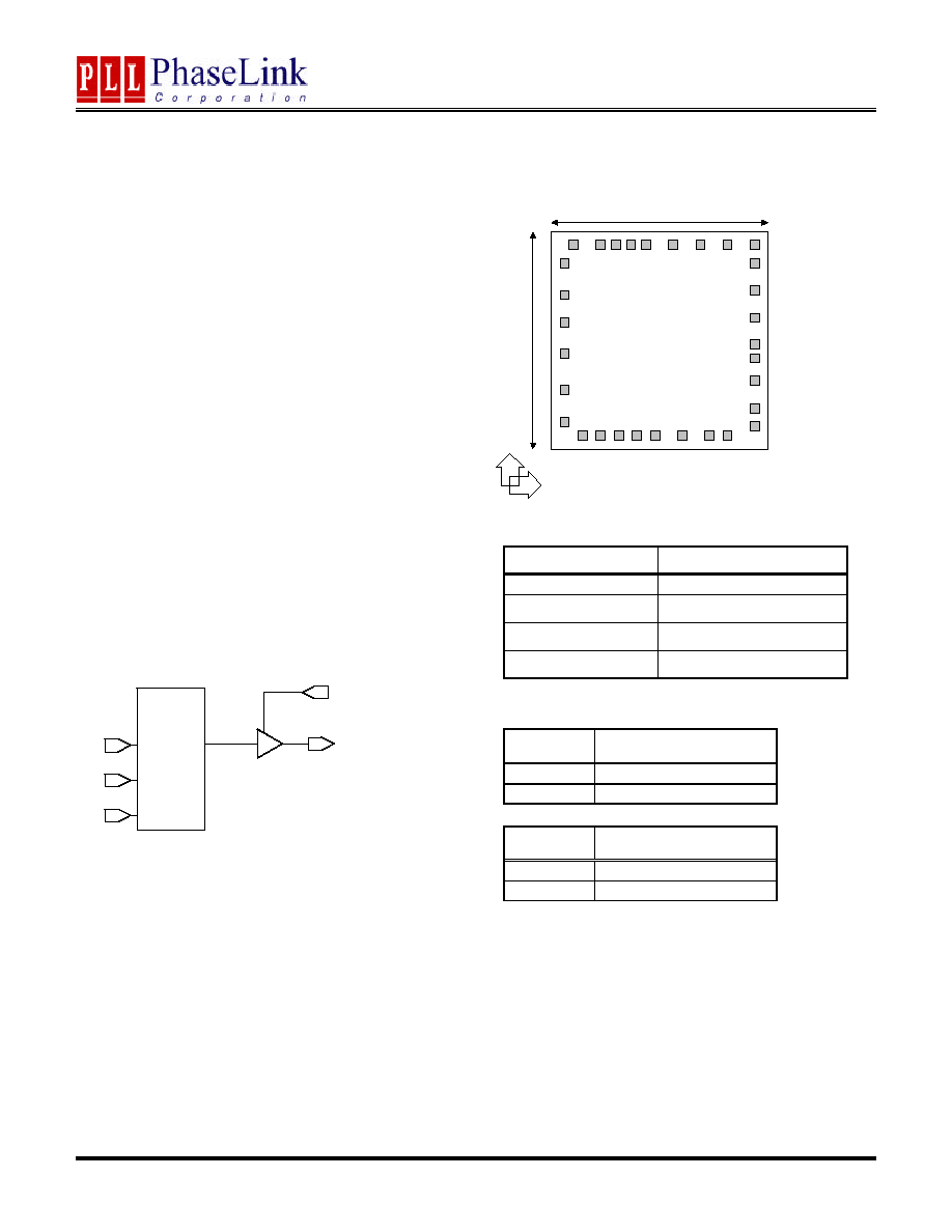
BLOCK DIAGRAM
DIE CONFIGURATION
DIE SPECIFICATIONS
Name
Value
Size
62 x 65 mil
Reverse side
GND
Pad dimensions
80 micron x 80 micron
Thickness
10 mil
DRIVE_SEL AND OE_CTRL TABLE
Pad #19
DRIVE_SEL
Output Drive
0
High Drive CMOS
1
Standard CMOS (default)
Pad #30
OE_CTRL
State
0
Tri-state
1
Output enabled (default)
18
19
20
21
23
25
7
13
10
26
29
31
Y
X
(0,0)
(1550,1475)
62 mil
65 mil
24
22
17
16
15
14
12
11
9
8
6
1
2
3
4
5
27
28
30
X+
X-
OE
Q
PLL520-70
VCON
Oscillator
Amplifier
w/
integrated
varicaps
Preliminary
PLL520-70
CMOS Low Phase Noise VCXO (for 45-90MHz Fund Xtal)
47745 Fremont Blvd., Fremont, California 94538 TEL (510) 492-0990 FAX (510) 492-0991 Rev 8/26/02 Page 2
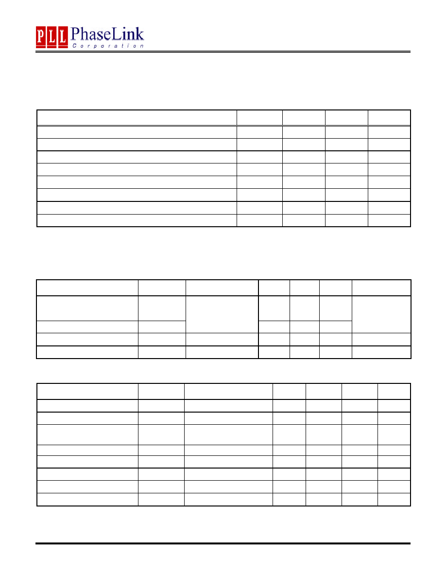
ELECTRICAL SPECIFICATIONS
1. Absolute Maximum Ratings
PARAMETERS
SYMBOL
MIN.
MAX.
UNITS
Supply Voltage
V
DD
7
V
Input Voltage, dc
V
I
V
SS
-0.5
V
DD
+0.5
V
Output Voltage, dc
V
O
V
SS
-0.5
V
DD
+0.5
V
Storage Temperature
T
S
-65
150
∞
C
Ambient Operating Temperature*
T
A
-40
85
∞
C
Junction Temperature
T
J
125
∞
C
Lead Temperature (soldering, 10s)
260
∞
C
Input Static Discharge Voltage Protection
2
kV
Exposure of the device under conditions beyond the limits specified by Maximum Ratings for extended periods may cause permanent damage to the
device and affect product reliability. These conditions represent a stress rating only, and functional operations of the device at these or any other
conditions above the operational limits noted in this specification is not implied.
* Note: Operating Temperature is guaranteed by design for all parts (COMMERCIAL and INDUSTRIAL), but tested for INDUSTRIAL grade only.
2. Crystal Specifications
3. Voltage Control Crystal Oscillator
PARAMETERS
SYMBOL
CONDITIONS
MIN.
TYP.
MAX.
UNITS
VCXO Stabilization Time *
T
VCXOSTB
From power valid
10
ms
VCXO Tuning Range
XTAL C
0
/C
1
< 250
200*
ppm
CLK output pullability
0V
VCON
3.3V
at room temperature
±
100*
ppm
On-chip Varicaps control range
VCON = 0 to 3.3V
4 ≠ 18*
pF
Linearity
5*
10*
%
VCXO Tuning Characteristic
65
ppm/V
VCON input impedance
60
k
VCON modulation BW
0V
VCON
3.3V, -3dB
25
kHz
Note:
Parameters denoted with an asterisk (*) represent nominal characterization data and are not production tested to any specific limits.
PARAMETERS
SYMBOL
CONDITIONS
MIN.
TYP.
MAX.
UNITS
CX+
2
Built-in Capacitance
CX-
2
Inter-electrode capacitance
C
0
45MHz to 90MHz
(VDD=3.3V)
3.6
pF
C0/C1 ratio (gamma)
250
-
Oscillation Frequency
OF
Fund.
45
90
MHz

Preliminary
PLL520-70
CMOS Low Phase Noise VCXO (for 45-90MHz Fund Xtal)
47745 Fremont Blvd., Fremont, California 94538 TEL (510) 492-0990 FAX (510) 492-0991 Rev 8/26/02 Page 3
4. General Electrical Specifications
PARAMETERS
SYMBOL
CONDITIONS
MIN.
TYP.
MAX.
UNITS
Supply Current (Loaded Outputs)
I
DD
40
mA
Operating Voltage
V
DD
3.13
3.47
V
Output Clock Duty Cycle
@ 1.4V
45
50
55
%
Short Circuit Current
±
50
mA
5. Jitter specifications
PARAMETERS
CONDITIONS
MIN.
TYP.
MAX. UNITS
Period jitter RMS
77.76MHz
3.5*
ps
Period jitter peak-to-peak
77.76MHz
24*
ps
Integrated jitter RMS
Integrated 12 kHz to 20 MHz at 77.76MHz
0.5*
ps
*: To be measured
6. Phase noise specifications
PARAMETERS
FREQUENCY
@10Hz
@100Hz @1kHz @10kHz @100kHz UNITS
Phase Noise relative to
carrier
77.76MHz
-75
-95
-125
-145
-155
dBc/Hz
Note: Phase Noise at VCON = 0V ≠ to be measured
7. CMOS Output Electrical Specifications
PARAMETERS
SYMBOL
CONDITIONS
MIN.
TYP. MAX. UNITS
Output High Voltage
V
OH
I
OH
= -12mA (Standard drive)
2.4
V
Output Low Voltage
V
OL
I
LO
= 12mA (Standard drive)
0.4
V
Output High Voltage at CMOS level
V
OHC
I
OH
= -4mA (Standard drive)
V
DD
≠ 0.4
V
At TTL level (High drive)
36
51
mA
Output drive current
At TTL level (Standard drive)
12
17
mA
8. CMOS Switching Characteristics
PARAMETERS
SYMBOL
CONDITIONS
MIN.
TYP. MAX. UNITS
0.8V ~ 2.0V with 10 pF load
1.15
Output Clock Rise/Fall Time
(Standard Drive)
0.3V ~ 3.0V with 15 pF load
3.7
0.8V ~ 2.0V with 10 pF load
0.5
Output Clock Rise/Fall Time
(High Drive)
0.3V ~ 3.0V with 15 pF load
1.5
ns
Preliminary
PLL520-70
CMOS Low Phase Noise VCXO (for 45-90MHz Fund Xtal)
47745 Fremont Blvd., Fremont, California 94538 TEL (510) 492-0990 FAX (510) 492-0991 Rev 8/26/02 Page 4
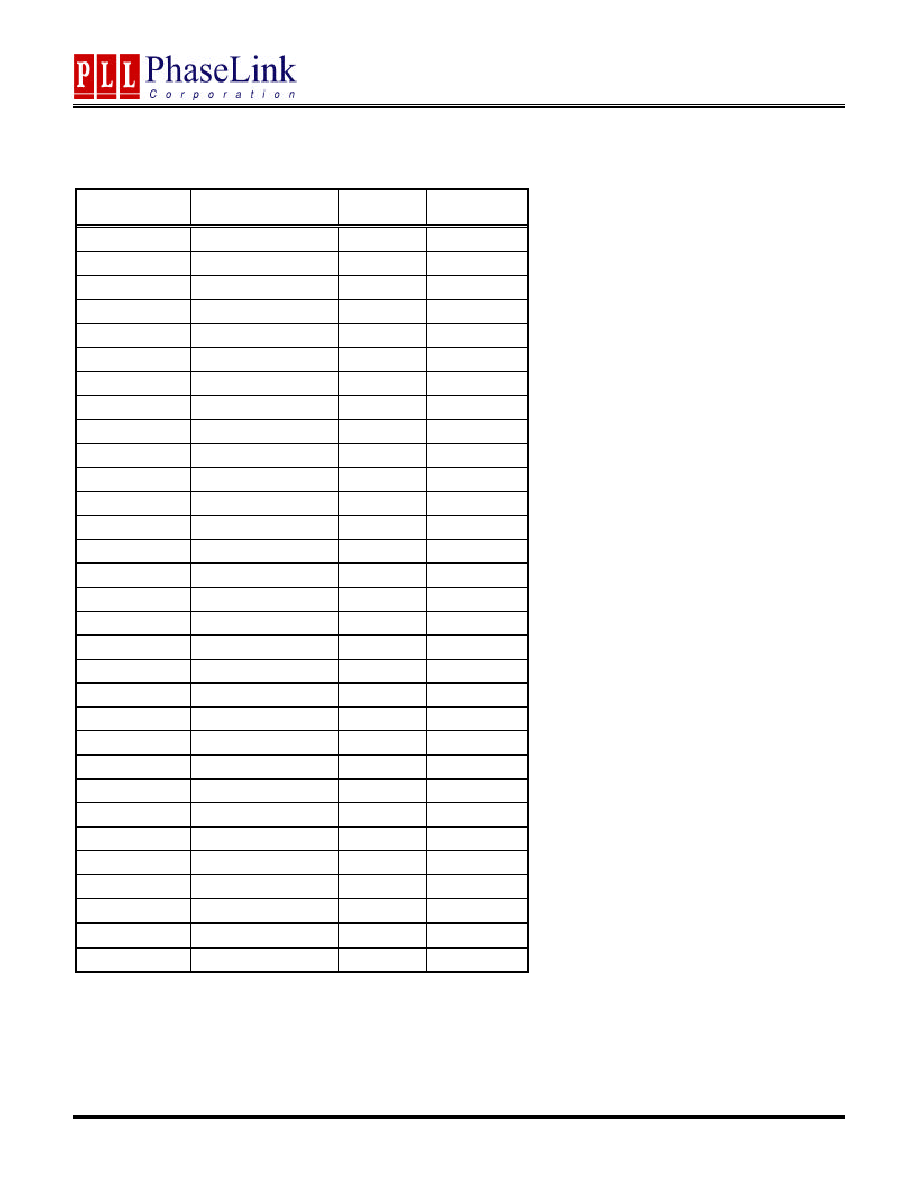
PAD ASSIGNMENT
Pad #
Name
X (
µ
µ
m)
Y (
µ
µ
m)
1
Optional GND
248
109
2
Optional GND
361
109
3
Optional GND
473
109
4
Optional GND
587
109
5
GND
702
109
6
Reserved
874
109
7
Optional GNDBUF
1042
109
8
Optional GNDBUF
1171
109
9
Not connected
1400
125
10
Not connected
1400
259
11
CMOS OUT
1400
476
12
VDDBUF
1400
616
13
Optional VDDBUF
1400
716
14
Not connected
1400
871
15
Not connected
1400
1089
16
Optional CMOS OUT
1400
1227
17
GNDBUF
1389
1365
18
Reserved
1232
1365
19
DRIVE_SEL
1042
1365
20
Not connected
854
1365
21
Optional VDD
659
1365
22
Optional VDD
559
1365
23
VDD
459
1365
24
Optional VDD
358
1365
25
Not connected
194
1365
26
XIN
109
1223
27
XOUT
109
1017
28
Not connected
109
858
29
Not connected
109
646
30
OE_CTRL
109
397
31
VCON
109
181
Note: for optimal Phase Noise performance, it is recommended to bond all optional VDD and GND pads.

Preliminary
PLL520-70
CMOS Low Phase Noise VCXO (for 45-90MHz Fund Xtal)
47745 Fremont Blvd., Fremont, California 94538 TEL (510) 492-0990 FAX (510) 492-0991 Rev 8/26/02 Page 5
ORDERING INFORMATION
PhaseLink Corporation, reserves the right to make changes in its products or specifications, or both at any time without notice. The information
furnished by Phaselink is believed to be accurate and reliable. However, PhaseLink makes no guarantee or warranty concerning the accuracy of said
information and shall not be responsible for any loss or damage of whatever nature resulting from the use of, or reliance upon this product.
LIFE SUPPORT POLICY: PhaseLink's products are not authorized for use as critical components in life support devices or systems without the
express written approval of the President of PhaseLink Corporation.
For part ordering, please contact our Sales Department:
47745 Fremont Blvd., Fremont, CA 94538, USA
Tel: (510) 492-0990 Fax: (510) 492-0991
PART NUMBER
The order number for this device is a combination of the following:
Device number, Package type and Operating temperature range
PLL520-70 D C
PART NUMBER
TEMPERATURE
C=COMMERCIAL
M=MILITARY
I=INDUSTRAL
PACKAGE TYPE
D=DIE