Preliminary
PLL520-88/-89
Low Phase Noise VCXO (9.5-65MHz)
47745 Fremont Blvd., Fremont, California 94538 Tel (510) 492-0990 Fax (510) 492-0991 www.phaselink.com Rev 09/20/04 Page 1
FEATURES
∑ 19MHz to 65MHz fundamental crystal input.
∑ Output range: 9.5MHz ≠ 65MHz
∑ Complementary outputs: PECL or LVDS output.
∑ Selectable OE Logic (enable high or enable low).
∑ Integrated variable capacitors.
∑ Supports 2.5V or 3.3V Power Supply.
∑ Available in 16 pin TSSOP package.
DESCRIPTION
The PLL520-88 (PECL) and PLL520-89 (LVDS) are
VCXO ICs specifically designed to work with
fundamental crystals between 19MHz and 65MHz.
The selectable divide by two feature extends the
operation range from 9.5MHz to 65MHz. They
require very low current into the crystal resulting in
better overall stability. The OE logic feature allows
selection of enable high or enable low.
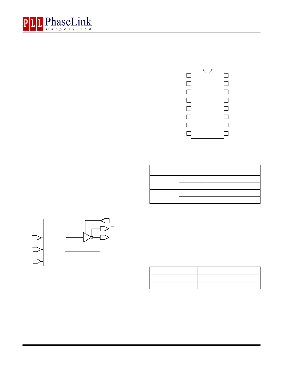
BLOCK DIAGRAM
PIN CONFIGURATION
OUTPUT SELECTION AND ENABLE
OE_SELECT OE_CTRL
State
0 Tri-state
0
1 (Default) Output enabled
0 (Default) Output enabled
1 (Default)
1 Tri-state
Input selection: Bond to GND to set to "0", bond to VDD to set to "1"
No connection results to "default" setting through
internal
pull-up/-down.
OE_CTRL:
Logical states defined by PECL levels if
OE_SELECT
is
"1"
Logical states defined by CMOS levels if
OE_SELECT
is
"0"
OUTPUT FREQUENCY DIVIDE BY
TWO SELECTOR
S2 Output
0 Intput/2
1 Input
O
Q
PLL520-8X Block Diagram
Q
Oscillator
Amplifier
with
Integrated
Varicaps
S2
VCON
X+
X-
P
L
L 520-8x
1
2
3
4
5
6
7
8
VDD
9
10
11
12
13
14
15
16
XIN
XOUT
DNC
S2
OE
VCON
GND
DNC
DNC
GNDBUF
QBAR
VDDBUF
Q
GNDBUF
GND
Preliminary
PLL520-88/-89
Low Phase Noise VCXO (9.5-65MHz)
47745 Fremont Blvd., Fremont, California 94538 Tel (510) 492-0990 Fax (510) 492-0991 www.phaselink.com Rev 09/20/04 Page 2
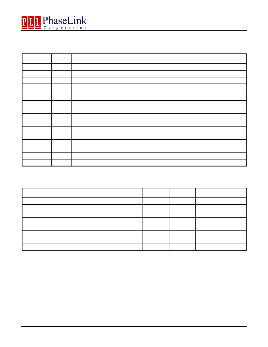
PIN AND PAD ASSIGNMENT
Name Pin#
Description
VDD 1
Power
Supply.
XIN
2
Crystal input. See Crystal Specification on page 3.
XOUT
3
Crystal output. See Crystal Specification on page 3.
DNC
4
Do Not Connect.
S2 5
Output Divide by Two selector pin. See the OUTPUT DIVIDE BY TWO SELECTOR Table on
page 1.
OE_CTRL
6
Output Enable input. See OUTPUT SELECTION AND ENABLE TABLE on page 1.
VCON
8
Voltage control input.
GND 9
Ground.
GNDBUF
10
Ground for output buffer circuitry.
Q
11
PECL or LVDS output.
VDDBUF
12
Power supply for output buffer circuitry.
QBAR
13
Complementary PECL or LVDS output.
GNDBUF
14
Ground for output buffer circuitry.
DNC
15
Do Not Connect.
DNC
16
Do Not Connect.
ELECTRICAL SPECIFICATIONS
1. Absolute Maximum Ratings
PARAMETERS SYMBOL
MIN.
MAX.
UNITS
Supply Voltage
V
DD
4.6 V
Input Voltage, dc
V
I
-0.5
V
DD
+0.5 V
Output Voltage, dc
V
O
-0.5
V
DD
+0.5 V
Storage Temperature
T
S
-65 150
∞C
Ambient Operating Temperature*
T
A
-40 85
∞C
Junction Temperature
T
J
125
∞C
Lead Temperature (soldering, 10s)
260
∞C
ESD Protection, Human Body Model
2
kV
Exposure of the device under conditions beyond the limits specified by Maximum Ratings for extended periods may cause permanent damage to the
device and affect product reliability. These conditions represent a stress rating only, and functional operations of the device at these or any other
conditions above the operational limits noted in this specification is not implied.
* Note: Operating Temperature is guaranteed by design for all parts (COMMERCIAL and INDUSTRIAL), but tested for COMMERCIAL grade only.
Preliminary
PLL520-88/-89
Low Phase Noise VCXO (9.5-65MHz)
47745 Fremont Blvd., Fremont, California 94538 Tel (510) 492-0990 Fax (510) 492-0991 www.phaselink.com Rev 09/20/04 Page 3
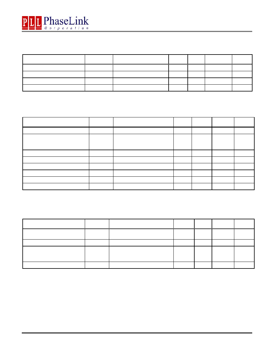
2. Crystal Specifications
PARAMETERS SYMBOL CONDITIONS MIN.
TYP.
MAX.
UNITS
Crystal Resonator Frequency
F
XIN
Fundamental
19
65 MHz
Crystal Loading Rating
C
L (xtal)
Die
8*
pF
Interelectrode Capacitance
C
0
5
pF
Recommended ESR
R
E
AT cut
30
Note: Parameters denoted with an asterisk (*) represent nominal characterization data and are not production tested to any specific
limits.
3. Voltage Control Crystal Oscillator (3.3V)
PARAMETERS SYMBOL CONDITIONS MIN.
TYP.
MAX.
UNITS
VCXO Stabilization Time *
T
VCXOSTB
From power valid
10
ms
VCXO Tuning Range
F
XIN
= 19 ≠ 65MHz;
XTAL C
0
/C
1
< 250
0V
VCON 3.3V
200* ppm
CLK output pullability
VCON=1.65V,
±1.65V
±100*
ppm
On-chip Varicaps control range
VCON = 0 to 3.3V
4 ≠ 18*
pF
Linearity
10*
%
VCXO Tuning Characteristic
65
ppm/V
VCON input impedance
60
k
VCON modulation BW
0V
VCON 3.3V, -3dB
25 kHz
Note: Parameters denoted with an asterisk (*) represent nominal characterization data and are not production tested to any specific
limits.
4. General Electrical Specifications
PARAMETERS SYMBOL CONDITIONS MIN.
TYP.
MAX.
UNITS
Supply Current (Loaded
Outputs)
I
DD
PECL/LVDS
100/80
mA
Operating Voltage
V
DD
2.97 3.63 V
Output Clock Duty Cycle
@ 50% V
DD
(CMOS)
@ 1.25V (LVDS)
@ V
DD
≠ 1.3V (PECL)
45
45
45
50
50
50
55
55
55
%
Short Circuit Current
±50
mA
Preliminary
PLL520-88/-89
Low Phase Noise VCXO (9.5-65MHz)
47745 Fremont Blvd., Fremont, California 94538 Tel (510) 492-0990 Fax (510) 492-0991 www.phaselink.com Rev 09/20/04 Page 4
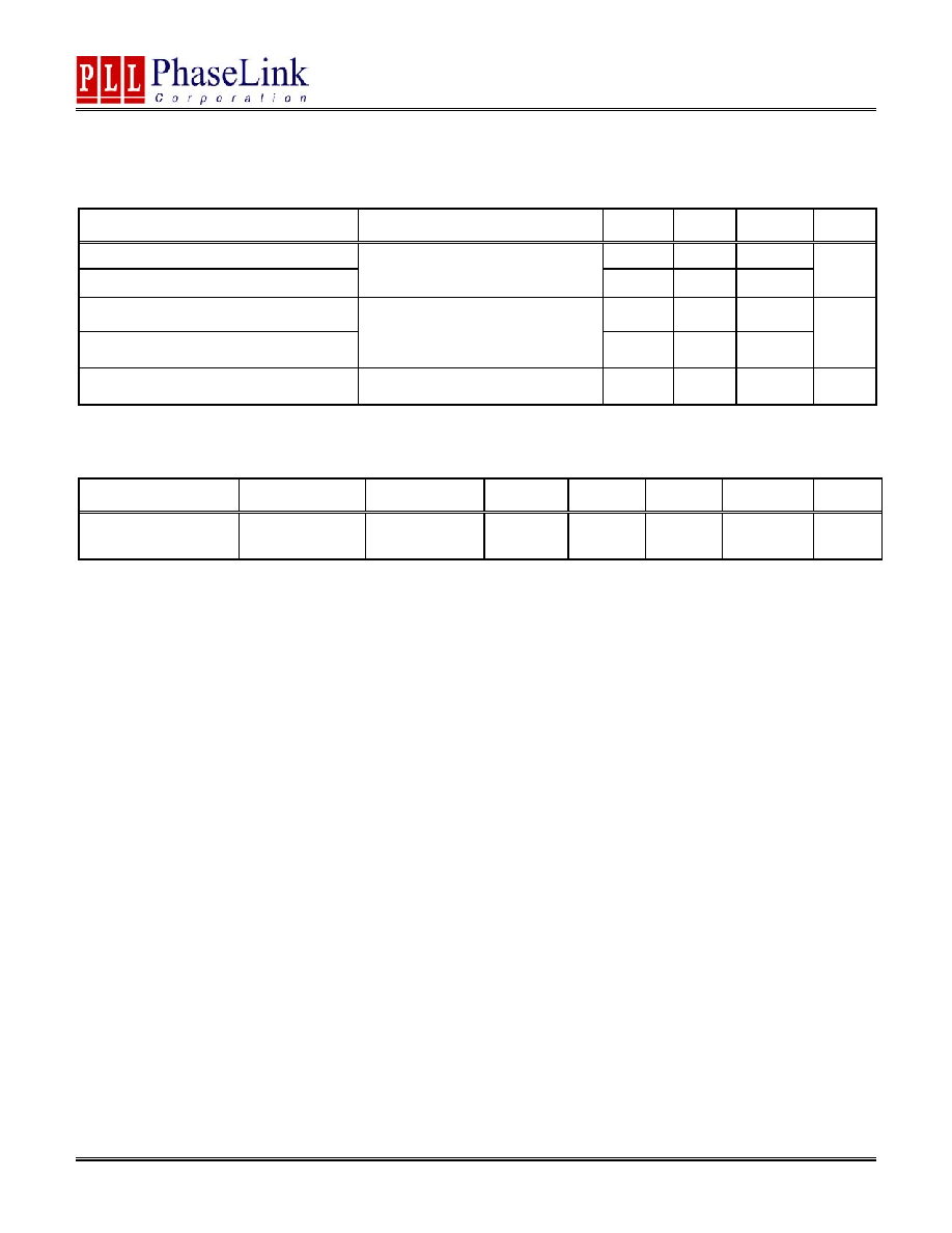
5. Jitter Specifications
PARAMETERS CONDITIONS
MIN.
TYP.
MAX.
UNITS
Period jitter RMS at 27MHz
2.3
Period jitter peak-to-peak at 27MHz
With capacitive decoupling
between VDD and GND. Over
10,000 cycles
18.5 20
ps
Accumulated jitter RMS at 27MHz
2.3
Accumulated jitter peak-to-peak at
27MHz
With capacitive decoupling
between VDD and GND. Over
1,000,000 cycles.
24 25
ps
Random Jitter
"RJ" measured on Wavecrest SIA
3000
2.3 ps
Measured on Wavecrest SIA 3000
6. Phase Noise Specifications
PARAMETERS FREQUENCY @10Hz
@100Hz @1kHz @10kHz @100kHz UNITS
Phase Noise relative
to carrier
27MHz -75
-100
-125
-140
-145
dBc/Hz
Note: Phase Noise measured on Agilent E5500
Preliminary
PLL520-88/-89
Low Phase Noise VCXO (9.5-65MHz)
47745 Fremont Blvd., Fremont, California 94538 Tel (510) 492-0990 Fax (510) 492-0991 www.phaselink.com Rev 09/20/04 Page 5
7. LVDS Electrical Characteristics
PARAMETERS SYMBOL
CONDITIONS
MIN.
TYP.
MAX.
UNITS
Output Differential Voltage
V
OD
247
355
454
mV
V
DD
Magnitude Change
V
OD
-50
50 mV
Output High Voltage
V
OH
1.4
1.6
V
Output Low Voltage
V
OL
0.9
1.1
V
Offset Voltage
V
OS
1.125
1.2
1.375
V
Offset Magnitude Change
V
OS
R
L
= 100
(see figure)
0
3 25 mV
Power-off Leakage
I
OXD
V
out
= V
DD
or GND
V
DD
= 0V
±1
±10
uA
Output Short Circuit Current
I
OSD
-5.7 -8
mA
8. LVDS Switching Characteristics
PARAMETERS SYMBOL
CONDITIONS
MIN.
TYP.
MAX.
UNITS
Differential Clock Rise Time
t
r
0.2 0.7 1.0 ns
Differential Clock Fall Time
t
f
R
L
= 100
C
L
= 10 pF
(see figure)
0.2 0.7 1.0 ns
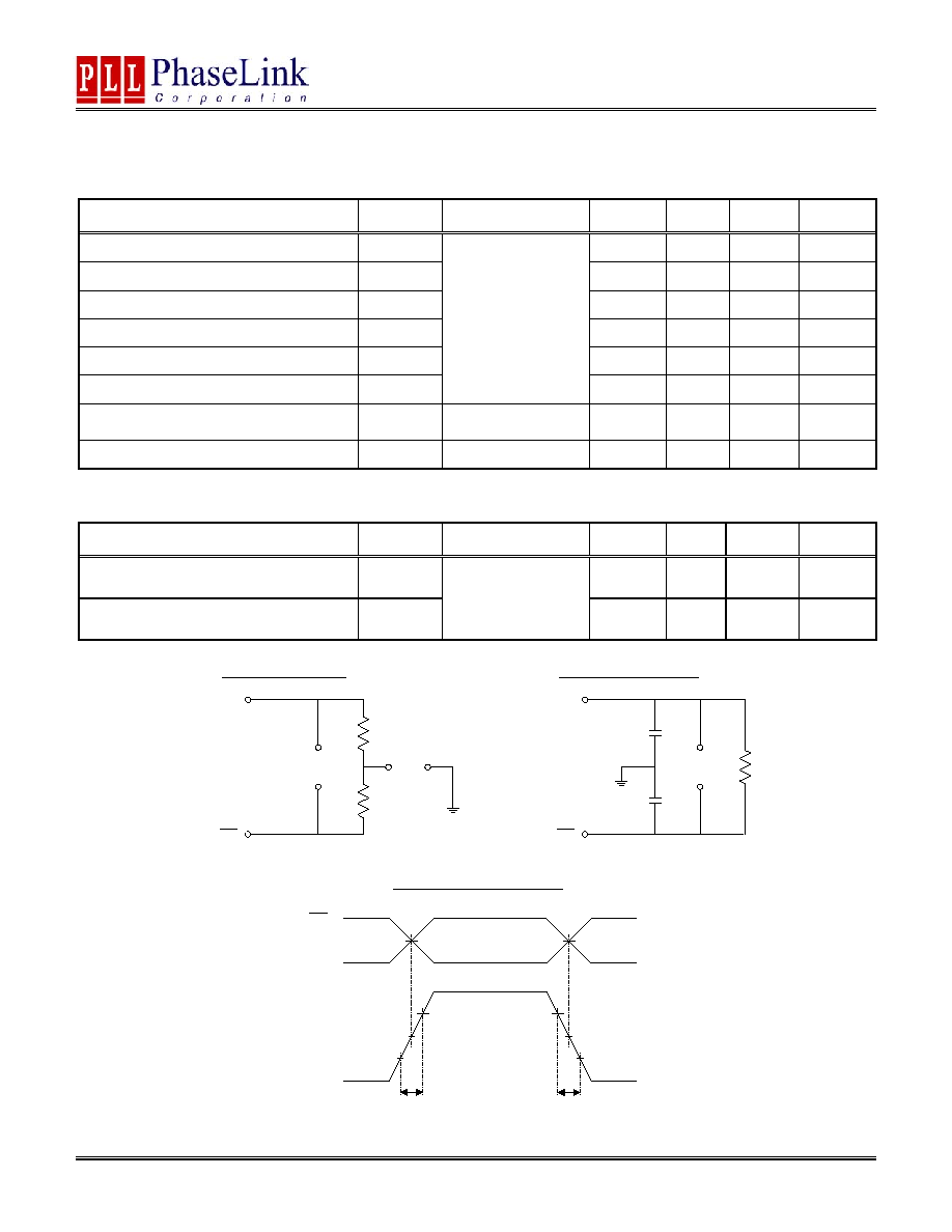
OUT
OUT
V
OD
V
OS
50
50
OUT
V
DIFF
R
L
= 100
C
L
= 10pF
C
L
= 10pF
LVDS Switching Test Circuit
LVDS Levels Test Circuit
LVDS Transistion Time Waveform
OUT
OUT
OUT
0V (Differential)
0V
20%
80%
20%
80%
t
R
t
F
V
DIFF