Preliminary
PLL600-27B
Ultra Low Current XO 10 MHz to 52 MHz
47745 Fremont Blvd., Fremont, California 94538 Tel (510) 492-0990 Fax (510) 492-0991 www.phaselink.com Rev 11/03/05 Page 1
FEATURES
∑ Low phase noise (-145 dBc @ 10kHz offset).
∑ CMOS output with OE tri-state control.
∑ Ultra Low current consumption ( <2mA, at
27MHz, 3.3V)
∑ 10 to 52MHz fundamental or 3
rd
OT crystal input.
∑ 12mA drive capability at TTL output.
∑ Low jitter (RMS): 2.5ps period jitter.
∑ 1.8V, 2.5V and 3.3V DC operation.
∑ Available in 8 pin SOIC
DESCRIPTION
The PLL600-27B form a low cost family of XO IC's,
designed to consume the lowest current on the mar-
ket for the 10MHz to 52MHz range. It accepts fun-
damental resonant mode crystal input from 10 to
52MHz. Providing less than -145 dBc at 10kHz offset
at 30MHz and with a very low jitter (2.5 ps RMS pe-
riod jitter) makes this chip ideal for applications re-
quiring low current frequency sources.
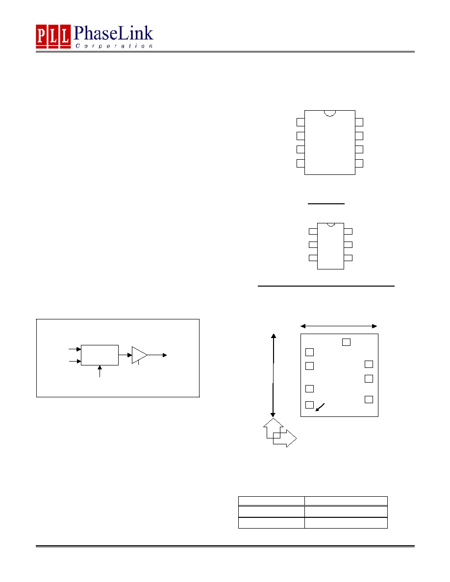
BLOCK DIAGRAM
PIN ASSIGNMENT (PACKAGE)
8-pin SOIC
PAD LAYOUT
OE LOGIC SELECTION TABLE
OE^ OUTPUT
0
Disabled - osc. off
1(default)
Enabled
SOT-23
1
2
3
4
5
6
GND
CLK
XOUT
XIN/FIN
OE^
VDD
P
L
L
6
00-27B
XTAL
OSC
XIN/FIN
XOUT
CLK
OE
OSCSEL
1
2
3
4
XIN/FIN
5
6
7
8
OE^
DNC
GND
XOUT
DNC
VDD
CLK
PL
L
600-2
7
B
^ : denotes internal pull-up
Y
X
(0,0)
39 m
i
l
32 mil
Die ID:
C500A-0505
-
05K
1
2
3
4
5
6
7
8
XOUT
DNC
VDD
CLK
XIN
OE
DNC
GND
(812, 986)
Preliminary
PLL600-27B
Ultra Low Current XO 10 MHz to 52 MHz
47745 Fremont Blvd., Fremont, California 94538 Tel (510) 492-0990 Fax (510) 492-0991 www.phaselink.com Rev 11/03/05 Page 2
^ Internal Pull-up, default value is `1' when not connected.
PACKAGE PIN DESCRIPTION
Pin No.
Pad
Type
Description
Name
SOIC-8
SOT-6 No.
X (
µm) Y
(
µm)
XIN/FIN
1
3
1
94.18
768.60
I
Crystal input or reference clock input pin.
OE
2
1
2
94.16
605.03
I
Output Enable input. See Table on page 1.
DNC
3
-
4
94.18
331.76
-
Do Not Connect.
GND 4 2 3
94.19
140.38
P
Ground
connection.
CLK 5 6 5
715.31
203.87
O
Output
clock.
VDD
6
5
6
715.31
455.73
P
Power supply connection.
DNC
7
-
7
715.47
626.72
-
Do Not Connect.
XOUT 8 4 8
476.91
888.88 O
Crystal
output.
OE has internal pull-up resistor, so the default value is `1' when not connected.
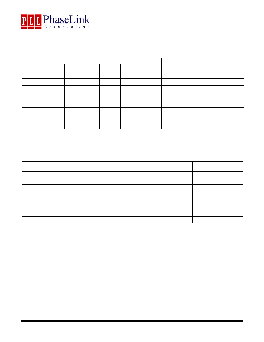
ELECTRICAL SPECIFICATIONS
1. Absolute Maximum Ratings
PARAMETERS SYMBOL
MIN.
MAX.
UNITS
Supply Voltage
V
DD
4.6 V
Input Voltage, dc
V
I
-0.5
V
DD
+0.5 V
Output Voltage, dc
V
O
-0.5
V
DD
+0.5 V
Storage Temperature
T
S
-65 150
∞C
Ambient Operating Temperature*
T
A
-40 85
∞C
Junction Temperature
T
J
125
∞C
Lead Temperature (soldering, 10s)
260
∞C
ESD Protection, Human Body Model
2
kV
Exposure of the device under conditions beyond the limits specified by Maximum Ratings for extended periods may cause permanent damage to the
device and affect product reliability. These conditions represent a stress rating only, and functional operations of the device at these or any other
conditions above the operational limits noted in this specification is not implied.
* Note: Operating Temperature is guaranteed by design for all parts (COMMERCIAL and INDUSTRIAL), but tested for COMMERCIAL grade only.
Preliminary
PLL600-27B
Ultra Low Current XO 10 MHz to 52 MHz
47745 Fremont Blvd., Fremont, California 94538 Tel (510) 492-0990 Fax (510) 492-0991 www.phaselink.com Rev 11/03/05 Page 3
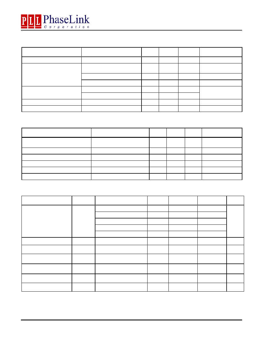
2. AC Electrical Specifications
PARAMETERS CONDITIONS
MIN.
TYP.
MAX.
UNITS
Input Crystal Frequency
10
52
MHz
At power-up
(Vdd reaches 1.62V)
10
ms
Disable to enable, osc. Off
10
ms
Settling time
Disable to enable, osc. On
500
µs
0.8V ~ 2.0V with 10 pF load
1.15
Output Clock Rise/Fall Time
0.3V ~ 3.0V with 15 pF load
2.4
ns
VDD sensitivity
Frequency vs. VDD +/- 10%
0.8
0.8
ppm
Output Clock Duty Cycle
Measured @ 50% V
DD
45
50
55 %
3. Jitter and Phase Noise Specifications
PARAMETERS CONDITIONS
MIN.
TYP.
MAX.
UNITS
RMS Period Jitter
(1 sigma ≠ 10,000 samples)
With capacitive decoupling
between VDD and GND.
2.1
2.5
ps
Phase Noise relative to carrier
27MHz @100Hz offset
-108
dBc/Hz
Phase Noise relative to carrier
27MHz @1kHz offset
-135
dBc/Hz
Phase Noise relative to carrier
27MHz @10kHz offset
-147
dBc/Hz
Phase Noise relative to carrier
27MHz @100kHz offset
-148
dBc/Hz
Phase Noise relative to carrier
27MHz @1MHz offset
-148
dBc/Hz
4. DC Specification
PARAMETERS SYMBOL CONDITIONS
MIN. TYP.
MAX. UNITS
At 10MHz, Cload=15pF
1.3
1.5
At 13.5MHz, Cload=15pF
1.5
1.7
At 17.7MHz, Cload=15pF
1.7
2.0
At 27MHz, Cload=15pF
2.3
2.7
Supply Current, Dynamic,
with Loaded Outputs
(at VDD = 3.3V)
I
DD
At 48MHz, Cload=15pF
4.0
4.6
mA
Operating Voltage
V
DD
1.62
3.63
V
Output High Voltage
V
OH
I
OH
= -12mA (3.3V)
2.4
V
Output Low Voltage
V
OL
I
OL
= 12mA (3.3V)
0.4
V
Output High Voltage at
CMOS level
V
OHC
I
OH
= -4mA
V
DD
≠ 0.4
V
Output drive current
At TTL level (3.3V)
12
17
mA
Short Circuit Current
(3.3V)
±50
mA
Preliminary
PLL600-27B
Ultra Low Current XO 10 MHz to 52 MHz
47745 Fremont Blvd., Fremont, California 94538 Tel (510) 492-0990 Fax (510) 492-0991 www.phaselink.com Rev 11/03/05 Page 4
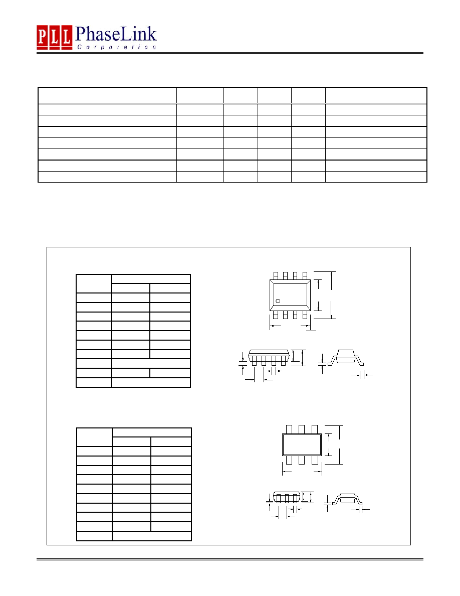
5. Crystal Specifications
PARAMETERS SYMBOL
MIN.
TYP.
MAX. UNITS
Crystal Resonator Frequency
F
XIN
10 52
MHz
Crystal Loading Rating
C
L (xtal)
8.5
pF
Maximum Sustainable Drive Level
200
µW
Operating Drive Level
50
µW
C0 (for frequencies below 30MHz)
5
pF
C0 (for frequencies above 30MHz)
4
pF
ESR R
S
30
Note: A detailed crystal specification document is also available for this part
PACKAGE INFORMATION
SOIC (8L)
SOT-23 (6L)
Dimension in MM
Symbol
Min. Max.
A 1.47 1.73
A1 0.1 0.25
A2
B 0.33 0.51
C
D 4.8 4.95
E 3.8 4.0
H 6.0
BSC
L 0.38 1.27
e 1.27
BSC
Dimension in MM
Symbol
Min. Max.
A 1.05 1.35
A1 0.05 0.15
A2 1.00 1.20
B 0.30 0.50
C 0.08 0.20
D 2.80 3.00
E 1.50 1.70
H 2.60 3.00
L 0.35 0.55
e 0.95
BSC
C
L
A2
E
H
D
A1
e
b
A
C
L
A2
E
H
D
A1
e
b
A

Preliminary
PLL600-27B
Ultra Low Current XO 10 MHz to 52 MHz
47745 Fremont Blvd., Fremont, California 94538 Tel (510) 492-0990 Fax (510) 492-0991 www.phaselink.com Rev 11/03/05 Page 5
ORDERING INFORMATION
PhaseLink Corporation, reserves the right to make changes in its products or specifications, or both at any time without notice. The information fur-
nished by Phaselink is believed to be accurate and reliable. However, PhaseLink makes no guarantee or warranty concerning the accuracy of said
information and shall not be responsible for any loss or damage of whatever nature resulting from the use of, or reliance upon this product.
LIFE SUPPORT POLICY: PhaseLink's products are not authorized for use as critical components in life support devices or systems without the ex-
press written approval of the President of PhaseLink Corporation.
For part ordering, please contact our Sales Department:
47745 Fremont Blvd., Fremont, CA 94538, USA
Tel: (510) 492-0990 Fax: (510) 492-0991
PART NUMBER
The order number for this device is a combination of the following:
Device number, Package type and Operating temperature range
PLL600-27B X X
X-R
Note: PhaseLink Supports GREEN Packaging
Part / Order Number
Marking
Package Option
PLL600-27BSC
P600-27BSC
8-Pin SOIC (Tube)
PLL600-27BSC-R
P600-27BSC
8-Pin SOIC (Tape and Reel)
PLL600-27BSCL P600-27BSCL
8-Pin SOIC (Tube), GREEN
PLL600-27BSCL-R P600-27BSCL 8-Pin
SOIC (Tape and Reel), GREEN
PLL600-27BTCL-R
P600-27BTC
6-Pin SOT (Tape and Reel)
PART NUMBER
TEMPERATURE
C=COMMERCIAL
I= INDUSTRIAL
PACKAGE TYPE
S=SOIC
T= SOT
NONE= NORMAL PACKAGE
L= GREEN PACKAGE
NONE= TUBE
R= TAPE AND REEL