 | –≠–ª–µ–∫—Ç—Ä–æ–Ω–Ω—ã–π –∫–æ–º–ø–æ–Ω–µ–Ω—Ç: PLL600-37 | –°–∫–∞—á–∞—Ç—å:  PDF PDF  ZIP ZIP |
Preliminary
PLL600-17/-27/-37
Ultra Low Current XO (Crystals from 10 MHz to 52 MHz)
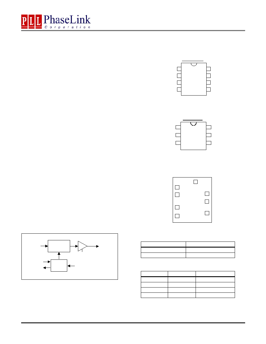
PIN ASSIGNMENT (PACKAGE)
FEATURES
8 pin SOIC
∑ Low phase noise (-130 dBc @ 10kHz offset).
1
2
3
4
XIN
5
6
7
8
SEL*^
GND
OSCSEL^
XOUT
OE^
VDD
CLK
P
LL60
0
-
x
7
* Note:
pin2 is SEL for PLL600-17
pin2 is N/C for PLL600-27/-37
^ :
denotes internal pull-up
∑ CMOS output with OE tri-state control.
∑ Selectable oscillator "on" or "off" feature in
output disable mode
∑ Ultra Low current consumption (<2.5mA, <2mA,
<1.3mA at 27MHz respectively for PLL600-17,
PLL600-27, and PLL600-37)
∑ Ultra Low disable mode current (<2uA when
disabled with osc. off)
∑ 10 to 52MHz fundamental crystal input.
6 pin SOT
∑ Selectable divider by 2 (PLL600-17 only).
∑ 12mA drive capability at TTL output.
PLL600-x7
1
2
3
4
5
6
CLK
GND
XIN
VDD
XOUT
OE^
^: denotes internal Pull-up
∑ Low jitter (RMS): 2.5ps period jitter.
∑ 2.25V to 3.63V DC operation.
∑ Available in 8 pin SOIC, 6 pin SOT or DIE.
DESCRIPTION
The PLL600-17/-27/-37 form a low cost family of XO
IC's, designed to consume the lowest current on the
market for the 5MHz to 52MHz range. It accepts
input crystal from 10 to 52MHz (fundamental
resonant mode) and offers a selectable divider by 2
(PLL600-17 only) or no division. Providing less than
-130dBc at 10kHz offset at 30MHz, and with a very
low jitter (2.5 ps RMS period jitter) makes this chip
ideal for applications requiring low current frequency
sources, such as handheld devices.
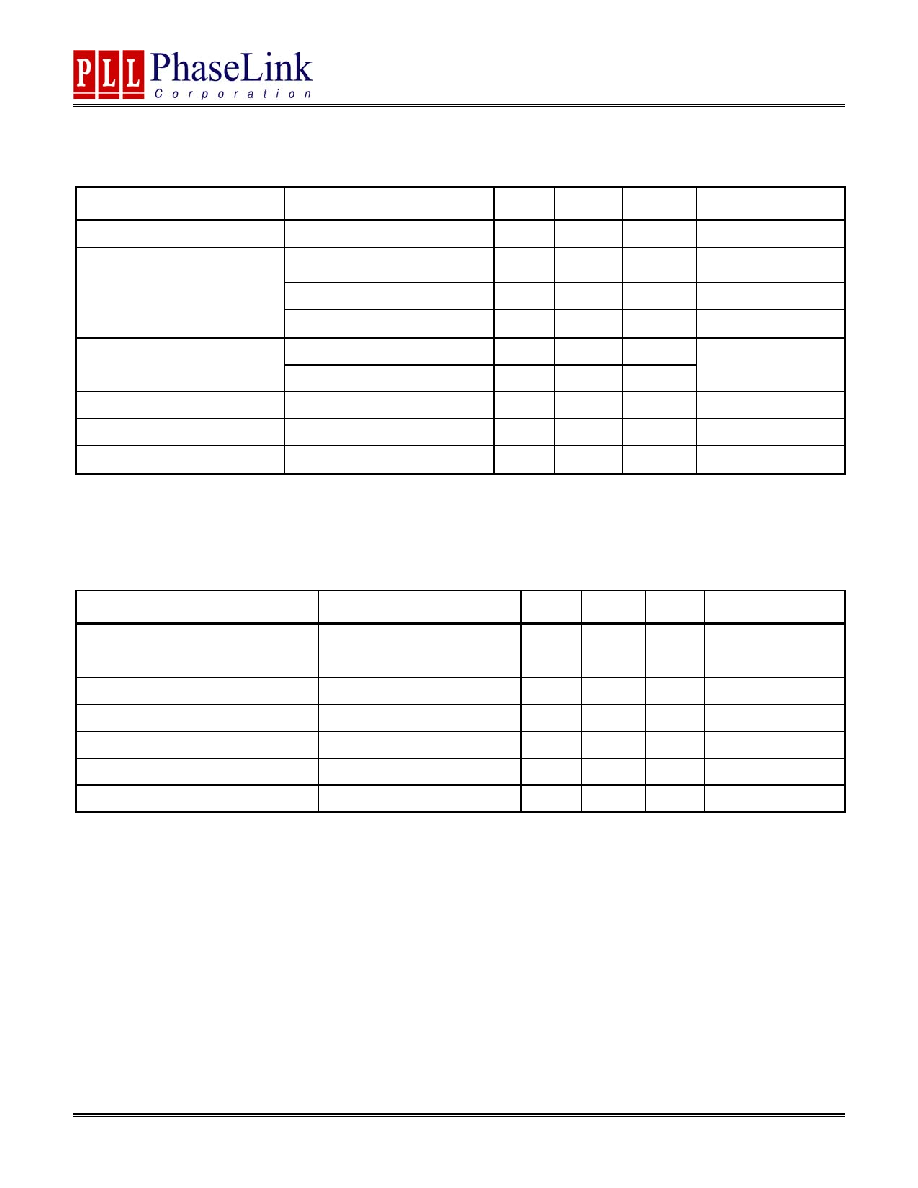
PAD ASSIGNMENT (DIE)
8
5
6
7
4
3
2
1
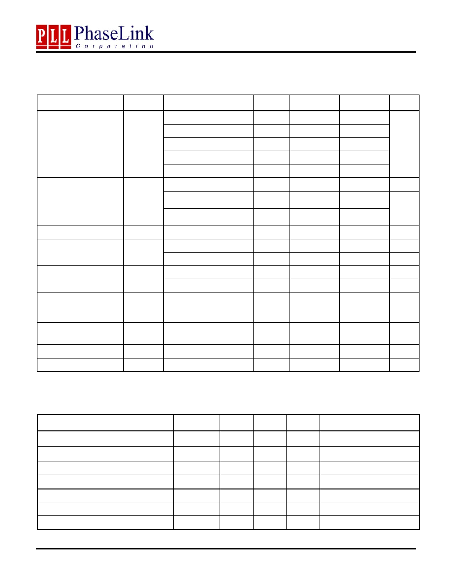
BLOCK DIAGRAM
SELECTION TABLE
Reference
Divider
XTAL
OSC
XIN
XOUT
CLK
SEL
OE
OSCSEL
SEL (PLL600-17 only)
DIVIDER
0 /
2
1 No
division
Internal Pull-up, default value is `1' when not connected.
Selectable divider only available on P600-17.
OE OSCSEL OUTPUT
0
0
Disabled - osc. off
0
1
Disabled - osc. on
1 0 Enabled
1 1 Enabled
Internal Pull-up, default value is `1' when not connected.
Not available in 6 pin SOT package.
47745 Fremont Blvd., Fremont, California 94538 TEL (510) 492-0990 FAX (510) 492-0991 Rev 9/23/03 Page 1
Preliminary
PLL600-17/-27/-37
Ultra Low Current XO (Crystals from 10 MHz to 52 MHz)
PIN DESCRIPTION
Pin #
Die Pad Position
Name
8 pin
6 pin
X (
µm) Y
(
µm)
Type Description
XOUT
1
4
94.183
768.599
I
Crystal output pin.
SEL 2 n/a
94.157 605.029 I
PLL600-17 only: select pin. See Table on page 1.
PLL600-27/-37: no connect
GND 3 2 94.183
331.756
P
Ground
pin.
OSCSEL
4
n/a
94.193
140.379
I
Disable mode select pin. See Table on page 1.
CLK
5
1
715.472
203.866
O
Output clock pin.
VDD
6
6
715.307
455.726
P
+3.3V VDD power supply pin.
OE
7
5
715.472
626.716
I
Output Enable input pin. See Table on page 1.
XIN
8
3
715.472
888.881
I
Crystal input pin.
SEL and OSCSEL have internal pull-ups, so the default value is `1' when not connected (not available on 6 pin package).
ELECTRICAL SPECIFICATIONS
1. Absolute Maximum Ratings
PARAMETERS SYMBOL
MIN.
MAX.
UNITS
Supply Voltage Range
V
CC
-
0.5
7 V
Input Voltage Range
V
I
-
0.5 V
CC
+
0.5
V
Output Voltage Range
V
O
-
0.5 V
CC
+
0.5
V
Soldering Temperature
260
∞C
Storage Temperature
T
S
-65 150
∞C
Ambient Operating Temperature*
0
70
∞C
Exposure of the device under conditions beyond the limits specified by Maximum Ratings for extended periods may cause permanent damage to the
device and affect product reliability. These conditions represent a stress rating only, and functional operations of the device at these or any other
conditions above the operational limits noted in this specification is not implied.
47745 Fremont Blvd., Fremont, California 94538 TEL (510) 492-0990 FAX (510) 492-0991 Rev 9/23/03 Page 2
Preliminary
PLL600-17/-27/-37
Ultra Low Current XO (Crystals from 10 MHz to 52 MHz)
2. AC Electrical Specifications
PARAMETERS CONDITIONS
MIN.
TYP.
MAX.
UNITS
Input Crystal Frequency
10
52
MHz
At power-up
(Vdd reaches 2.2V)
10*
ms
Disable to enable, osc. Off
10*
ms
Settling time
Disable to enable, osc. On
500*
µs
0.8V ~ 2.0V with 10 pF load
1.15
Output Clock Rise/Fall Time
0.3V ~ 3.0V with 15 pF load
3.7
ns
VDD sensitivity
Frequency vs. VDD +/- 10%
0.8
0.8
ppm
Output Clock Duty Cycle
Measured @ 1.4V
45
50
55
%
Short Circuit Current
±50
mA
Note: (*) Preliminary Specifications still to be characterized.
3. Jitter and Phase Noise specification
PARAMETERS CONDITIONS
MIN.
TYP.
MAX.
UNITS
RMS Period Jitter
(1 sigma ≠ 1000 samples)
With capacitive decoupling
between VDD and GND.
2.1
2.5
ps
Phase Noise relative to carrier
30MHz @100Hz offset
-80
dBc/Hz
Phase Noise relative to carrier
30MHz @1kHz offset
-110
dBc/Hz
Phase Noise relative to carrier
30MHz @10kHz offset
-130
dBc/Hz
Phase Noise relative to carrier
30MHz @100kHz offset
-138
dBc/Hz
Phase Noise relative to carrier
30MHz @1MHz offset
-145
dBc/Hz
47745 Fremont Blvd., Fremont, California 94538 TEL (510) 492-0990 FAX (510) 492-0991 Rev 9/23/03 Page 3
Preliminary
PLL600-17/-27/-37
Ultra Low Current XO (Crystals from 10 MHz to 52 MHz)
4. DC Specification
PARAMETERS SYMBOL CONDITIONS
MIN. TYP.
MAX. UNITS
At 10MHz, Cload=15pF
1.3 / 1 / 0.75
1.4 / 1.1 / 0.9
At 13.5MHz, Cload=15pF
1.5 / 1.2 / 0.8
1.6 / 1.3 / 1
At 17.7MHz, Cload=15pF
1.8 / 1.5 / 1
1.9 / 1.6 / 1.1
At 27MHz, Cload=15pF
2.4 / 2 / 1.2
2.5 / 2.1 / 1.3
Supply Current, Dynamic,
with Loaded Outputs
(at VDD = 3.3V)
Respectively for PLL600
-17/-27/-37
I
DD
At 48MHz, Cload=15pF
4.1 / 3.5 / 2.1 4.2 / 3.6 / 2.2
mA
Output disabled, Osc. off
2 4
µA
Output disabled, Osc. On
(PLL600-17)
620
Supply Current in tri-
state
I
DD
Output disabled, Osc. On
(PLL600-27/-37)
520
µA
Operating Voltage
V
DD
2.25
3.63
V
I
OH
= -12mA*
2.4
V
Output High Voltage
V
OH
PLL600-37*, I
OH
= -12mA*
2.4
2.9
V
I
OL
= 12mA*
0.4
V
Output Low Voltage
V
OL
PLL600-37*, I
OL
= 12mA*
0.32
0.4
V
Output High Voltage at
CMOS level (PLL600-17/
-27)
V
OHC
I
OH
= -4mA
V
DD
≠ 0.4
V
Output drive current
(PLL600-17/-27)
At TTL level
12
17
mA
Short Circuit Current
±50
mA
ESD Protection
Human Body Model
3000
V
* Note: PLL600-37 has non-standard CMOS VOH and VOL levels for lower current consumption, but meets CMOS input stage needs. PLL600-37
should be used to drive pure capacitive loads only.
5. Crystal Specifications
PARAMETERS SYMBOL
MIN.
TYP.
MAX. UNITS
Crystal Resonator Frequency
F
XIN
10 52
MHz
Crystal Loading Rating
C
L
(xtal)
8.5
pF
Maximum Sustainable Drive Level
200
µW
Operating Drive Level
50
µW
C0 (for frequencies below 30MHz)
5
pF
C0 (for frequencies above 30MHz)
4
pF
ESR R
S
30
Note: A detailed crystal specification document is also available for this part
47745 Fremont Blvd., Fremont, California 94538 TEL (510) 492-0990 FAX (510) 492-0991 Rev 9/23/03 Page 4
Preliminary
PLL600-17/-27/-37
Ultra Low Current XO (Crystals from 10 MHz to 52 MHz)
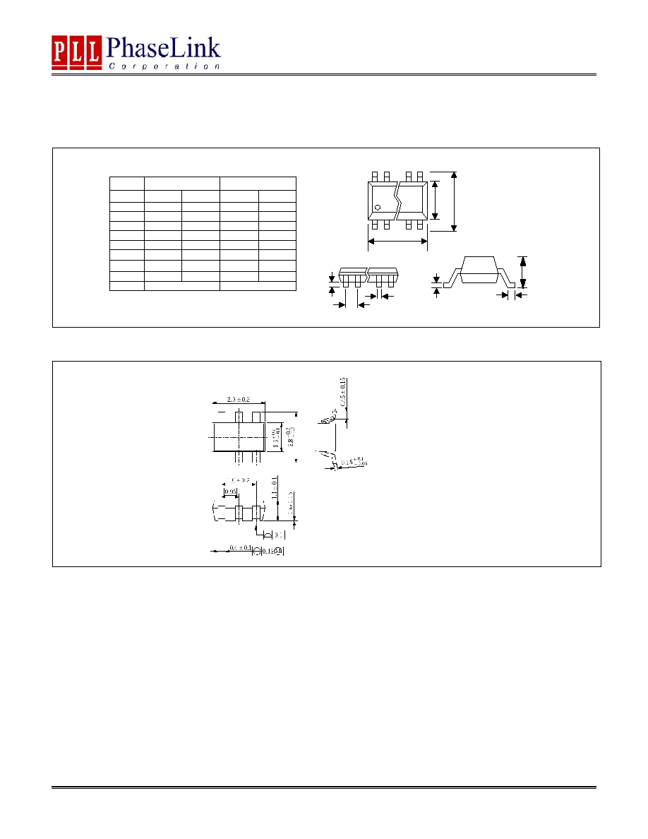
PACKAGE INFORMATION
C
L
A
8 PIN ( dimensions in mm )
Narrow SOIC
Symbol
Min.
Max.
A
1.47
1.73
A1
0.10
0.25
B
0.33
0.51
C
0.19
0.25
D
4.80
4.95
E
3.80
4.00
H
5.80
6.20
L
0.38
1.27
e
1.27 BSC
E
H
D
A1
e
B
TSSOP
Min.
Max.
-
1.20
0.05
0.15
0.19
0.30
0.09
0.20
2.90
3.10
4.30
4.50
6.20
6.60
0.45
0.75
0.65 BSC
6 PIN SOT (dimensions in mm)
47745 Fremont Blvd., Fremont, California 94538 TEL (510) 492-0990 FAX (510) 492-0991 Rev 9/23/03 Page 5