Preliminary
PLL601-03
Low Phase Noise PLL Clock Multiplier
47745 Fremont Blvd., Fremont, California 94538 TEL (510) 492-0990 FAX (510) 492-0991 Rev 06/15/01 Page 1
FEATURES
∑
Full swing CMOS outputs with 25 mA drive
capability at TTL levels.
∑
Reference 10-30MHz crystal or clock.
∑
Integrated crystal load capacitor: no external
load capacitor required.
∑
Output clocks up to 198MHz at 3.3V.
∑
Low phase noise (-126dBc/Hz @ 1kHz).
∑
Output Enable function.
∑
Low jitter (RMS): 6.4ps (period), 9.4ps (accum.)
∑
Advanced low power sub-micron CMOS process.
∑
3.3V operation.
∑
Available in 16-Pin SOIC or TSSOP.
DESCRIPTIONS
The PLL601-03 is a low cost, high performance and
low phase noise clock synthesizer. It implements
PhaseLink's proprietary analog and digital Phase
Locked Loop techniques to allow the user to select
the desired multiplier value. The chip accepts crystal
or clock inputs ranging from 10 to 30MHz, depening
on selected multiplier, and produces outputs clocks
up to 198MHz at 3.3V.
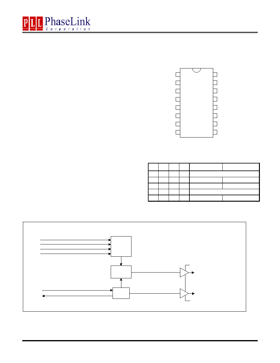
BLOCK DIAGRAM
PIN CONFIGURATION
MULTIPLIER SELECT TABLE
S3 S2 S1 S0
Multiplier
Xtal range
0
0
0
0
Reserved
0
0
0
1
11x
10≠18MHz
0
1
0
1
5x
20-30MHz
1
0
0
1
Frequency Pass through
1
1
0
1
6x
11-22MHz
PLL 601-03
1
2
3
4
5
6
7
8
CLK
9
10
11
12
13
14
15
16
REFEN
VDD
VDD
VDD
XOUT
S1
XIN
GND
GND
GND
REFOUT
OE
S0
S3
S2
Phase
Locked
Loop
ROM Based
Multipliers
XTAL
OSC
CLK
REFOUT
OE
REFEN
S2
S1
S0
XIN
XOUT
S3
Preliminary
PLL601-03
Low Phase Noise PLL Clock Multiplier
47745 Fremont Blvd., Fremont, California 94538 TEL (510) 492-0990 FAX (510) 492-0991 Rev 06/15/01 Page 2
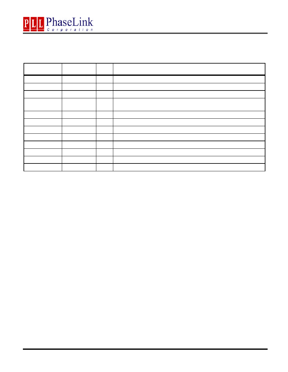
PIN DESCRIPTIONS
Name
Number
Type
Description
CLK
1
O Clock output from VCO. Equals the input frequency times multiplier.
REFEN
2
I
Reference clock enable. When Low, it turns off REFOUT.
VDD
3,4,5
P
3.3V Power Supply.
XIN
8
I
Crystal input to be connected to 10-30MHz fundamental parallel mode crys-
tal (C
L
=15pF). On chip load capacitors: No external capacitor required.
XOUT
6
O
Crystal Connection.
OE
12
I
Output Enable. Tri-state CLK and REFOUT when low. Has internal pull-up.
REFOUT
13
O
Buffered crystal oscillator clock output. Controlled by REFEN.
S0
11
I
Multiplier Select Pin 0. Determines CLK output. Has internal pull-up.
S1
7
I
Multiplier Select Pin 1. Determines CLK output. Has internal pull-up.
S2
9
I
Multiplier Select Pin 1. Determines CLK output. Has internal pull-up.
S3
10
I
Multiplier Select Pin 3. Determines CLK output. Has internal pull-up.
GND
14,15,16
P
Ground.
Preliminary
PLL601-03
Low Phase Noise PLL Clock Multiplier
47745 Fremont Blvd., Fremont, California 94538 TEL (510) 492-0990 FAX (510) 492-0991 Rev 06/15/01 Page 3
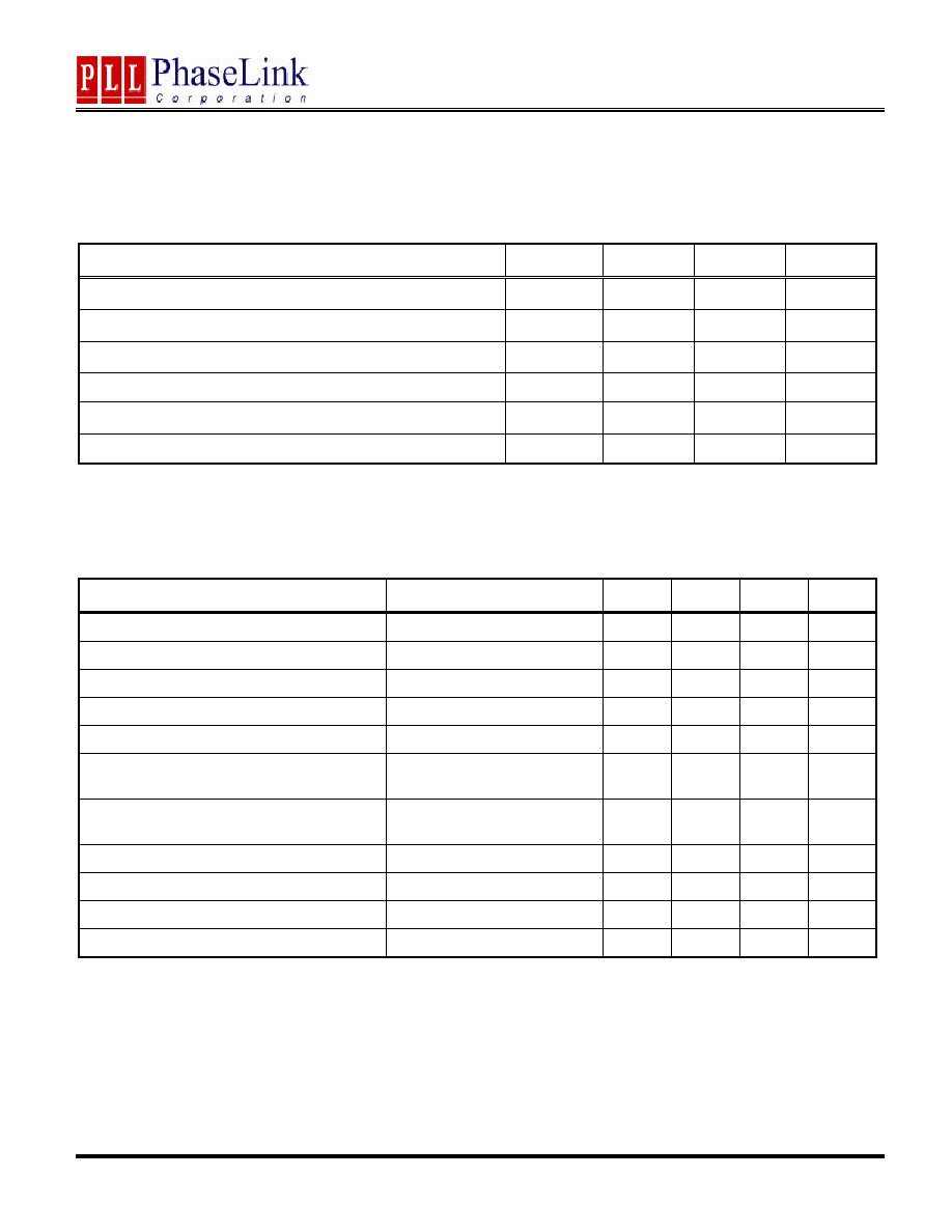
ELECTRICAL SPECIFICATIONS
1. Absolute Maximum Ratings
PARAMETERS
SYMBOL
MIN.
MAX.
UNITS
Supply Voltage Range
V
CC
-
0.5
7
V
Input Voltage Range
V
I
-
0.5
V
CC
+
0.5
V
Output Voltage Range
V
O
-
0.5
V
CC
+
0.5
V
Soldering Temperature
260
∞
C
Storage Temperature
T
S
-65
150
∞
C
Ambient Operating Temperature
0
70
∞
C
Exposure of the device under conditions beyond the limits specified by Maximum Ratings for extended periods may cause permanent damage to the
device and affect product reliability. These conditions represent a stress rating only, and functional operations of the device at these or any other con-
ditions above the operational limits noted in this specification is not implied.
2. AC Specification
PARAMETERS
CONDITIONS
MIN.
TYP.
MAX. UNITS
Input Frequency
Depends on selected multiplier
10
30
MHz
Output Frequency
At 3.3V
160
MHz
Output Rise Time
0.8V to 2.0V with no load
1.5
ns
Output Fall Time
2.0V to 0.8V with no load
1.5
ns
Duty Cycle
At VDD/2
45
50
55
%
Period jitter RMS
With capacitive decoupling
between VDD and GND
6.4
ps
Accumulated jitter RMS
With capacitive decoupling
between VDD and GND
9.4
ps
Phase Noise, relative to carrier, 155Mhz(x8) 100Hz offset, 3.3V
-103
dBc/Hz
Phase Noise, relative to carrier, 155Mhz(x8) 1kHz offset, 3.3V
-126
dBc/Hz
Phase Noise, relative to carrier, 155Mhz(x8) 10kHz offset, 3.3V
-133
dBc/Hz
Phase Noise, relative to carrier, 155Mhz(x8) 100kHz offset, 3.3V
-128
dBc/Hz
Preliminary
PLL601-03
Low Phase Noise PLL Clock Multiplier
47745 Fremont Blvd., Fremont, California 94538 TEL (510) 492-0990 FAX (510) 492-0991 Rev 06/15/01 Page 4
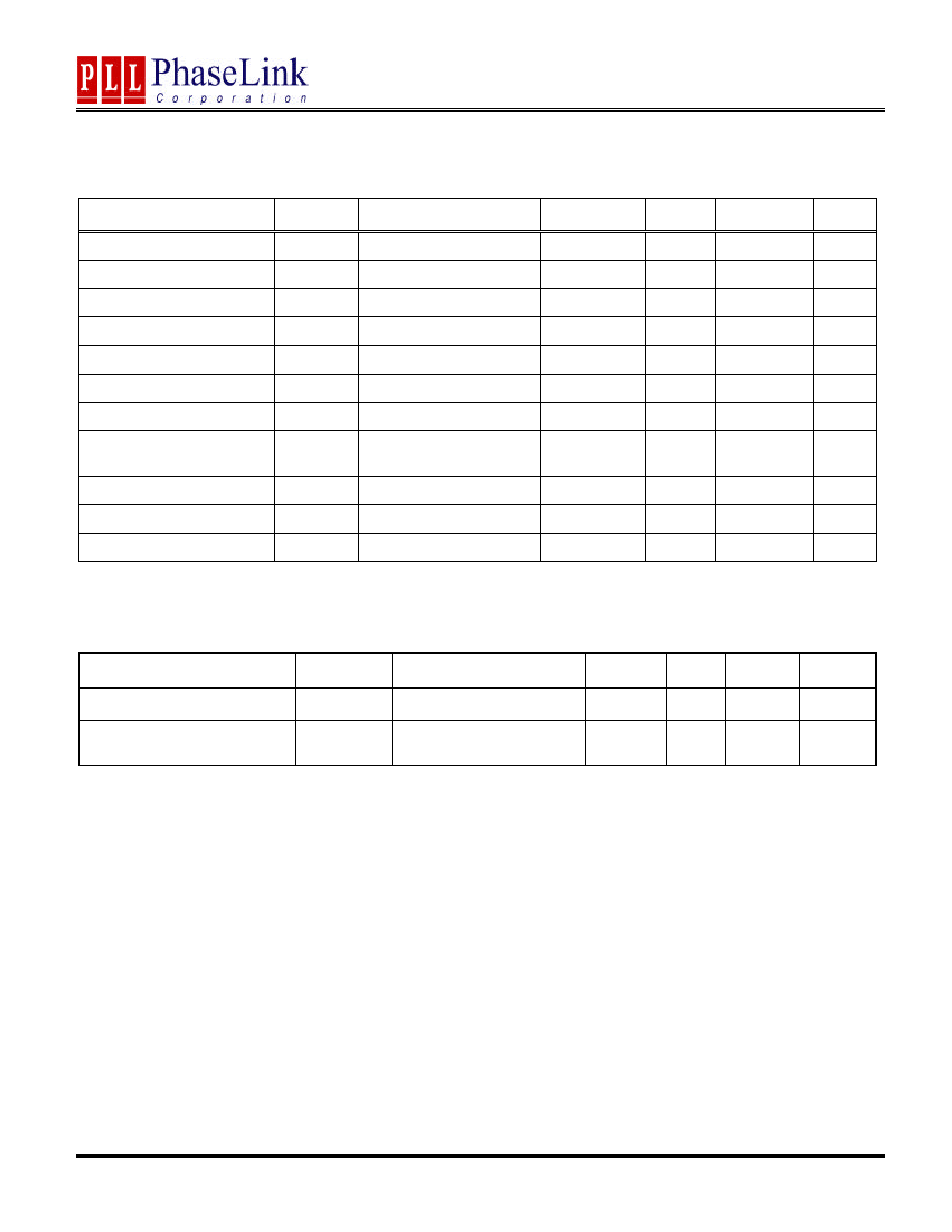
3. DC Specification
PARAMETERS
SYMBOL
CONDITIONS
MIN.
TYP.
MAX.
UNITS
Operating Voltage
VDD
3.135
3.465
V
Input High Voltage
V
IH
2
V
Input Low Voltage
V
IL
0.8
V
Input High Voltage
V
IH
For XIN pin
(VDD/2)
+
1
VDD/2
V
Input Low Voltage
V
IL
For XIN pin
VDD/2 (VDD/2)
-
1
V
Output High Voltage
V
OH
I
OH
= -25mA
2.4
V
Output Low Voltage
V
OL
I
OL
= 25mA
0.4
V
Output High Voltage At
CMOS Level
V
OH
I
OH
= -8mA
VDD-0.4
V
Operating Supply Current
I
DD
No Load
35
mA
Short-circuit Current
I
S
±
120
mA
Input Capacitance
C
IN
OE, Select Pins
5
pF
4. Crystal Specifications
PARAMETERS
SYMBOL
CONDITIONS
MIN.
TYP.
MAX.
UNITS
Crystal Resonator Frequency
F
XIN
Parallel Fundamental Mode
10
30
MHz
Crystal Loading Capacitance
Rating
C
L
(xtal)
15
pF
Preliminary
PLL601-03
Low Phase Noise PLL Clock Multiplier
47745 Fremont Blvd., Fremont, California 94538 TEL (510) 492-0990 FAX (510) 492-0991 Rev 06/15/01 Page 5
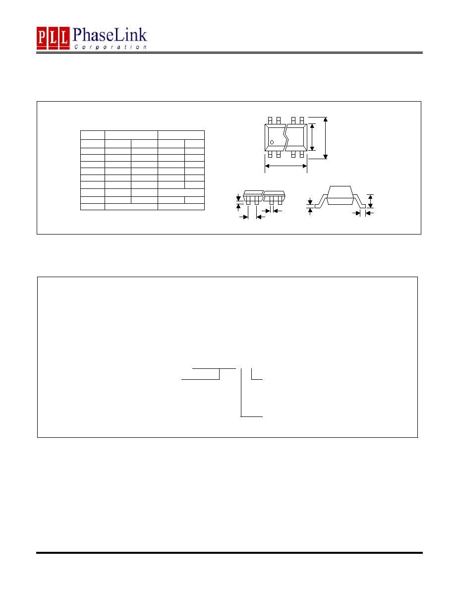
PACKAGE INFORMATION
ORDERING INFORMATION
PhaseLink Corporation, reserves the right to make changes in its products or specifications, or both at any time without notice. The information fur-
nished by Phaselink is believed to be accurate and reliable. However, PhaseLink makes no guarantee or warranty concerning the accuracy of said
information and shall not be responsible for any loss or damage of whatever nature resulting from the use of, or reliance upon this product.
LIFE SUPPORT POLICY
: PhaseLink's products are not authorized for use as critical components in life support devices or systems without the ex-
press written approval of the President of PhaseLink Corporation.
For part ordering, please contact our Sales Department:
47745 Fremont Blvd., Fremont, CA 94538, USA
Tel: (510) 492-0990 Fax: (510) 492-0991
PART NUMBER
The order number for this device is a combination of the following:
Device number, Package type and Operating temperature range
PLL601-03 X C
PART NUMBER
TEMPERATURATURE
C=COMMERCIAL
M=MILITARY
I=INDUSTRAL
PACKAGE TYPE
S=SOIC, O=TSSOP
C
L
A
16 PIN Narrow SOIC, TSSOP ( mm )
SOIC
TSSOP
Symbol
Min.
Max.
Min.
Max.
A
1.35
1.75
-
1.20
A1
0.10
0.25
0.05
0.15
B
0.33
0.51
0.19
0.30
C
0.19
0.25
0.09
0.20
D
9.80
10.00
4.90
5.10
E
3.80
4.00
4.30
4.50
H
5.80
6.20
6.40 BSC
L
0.40
1.27
0.45
0.75
e
1.27 BSC
0.65 BSC
E
H
D
A1
e
B