Preliminary
PLL601-26
Audio Clock Generator
47745 Fremont Blvd., Fremont, California 94538 Tel (510) 492-0990 Fax (510) 492-0991 www.phaselink.com Rev 11/28/05 Page 1
FEATURES
∑
Supports the following output frequencies
o
12.288MHz audio clock output
o
24.576MHz audio clock output
o
27MHz reference output
∑
Accepts Crystal or reference clock inputs
o
Fundamental crystal: 27MHz
o
Reference input: 27MHz
∑
On-the-fly switching of the two audio frequencies
(12.288MHz, and 24.576MHz).
∑
Accepts <1.0V reference signal input voltage
∑
Single 2.5V or 3.3V ± 10% power supply
∑
Available in 8-Pin SOIC GREEN/RoHS compliant
Package.
DESCRIPTION
The PLL601-26 is a low cost integrated XO IC
designed to work with a fundamental 27MHz crystal
or a clock input. In addition to a 27MHz clock
reference output, it provides two selectable audio
frequencies (12.288MHz, and 24.576MHz), making
the chip ideal for handheld, STB and MPEG Video
applications. Additional system frequencies can also
be supported by cascading the PLL601-26 with
PhaseLink's QTC programmable clock family.
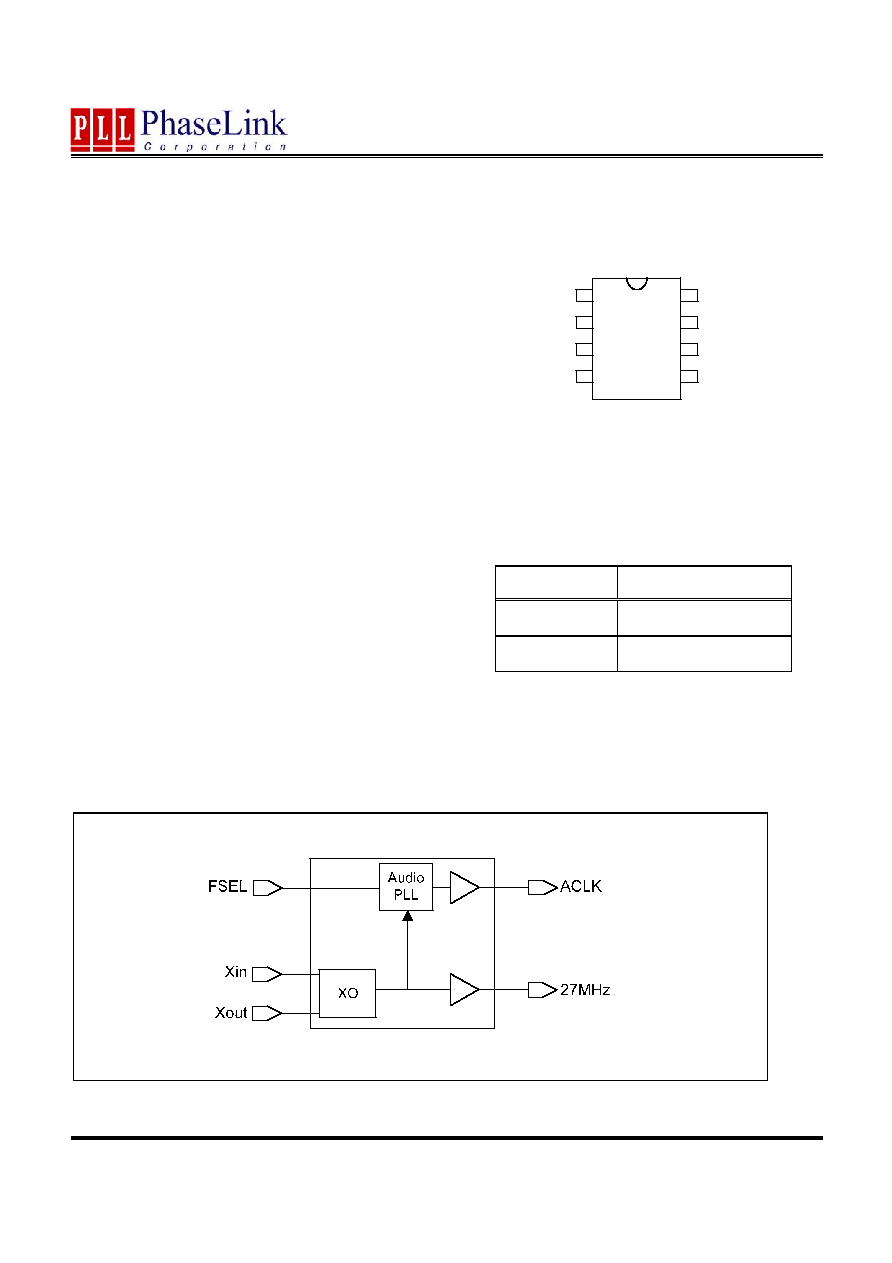
PACKAGE PIN CONFIGURATION
Note: ^: Internal pull-up resistor. The internal pull-up resistor
results in a default high value when no pull-down resistor is
connected to this pin.
AUDIO CLOCK SELECTION
FSEL
ACLK (MHz)
0 12.288
1(Default) 24.576
BLOCK DIAGRAM
PL
L
601-
2
6
1
2
3
4
5
6
7
8
XOUT
VDD
GND
27MHz
XIN/FIN
DNC
ACLK
FSEL^
Preliminary
PLL601-26
Audio Clock Generator
47745 Fremont Blvd., Fremont, California 94538 TEL (510) 492-0990 FAX (510) 492-0991 www.phaselink.com Rev 11/28/05 Page 2
PIN DESCRIPTIONS
Name Pin
# Type
Description
XIN/FIN
1
I
27Mhz Crystal or Reference input.
VDD 2 P
Power
supply
connection.
GND 3 P
Ground
connection.
27MHz 4 O
27MHz
reference
output.
ACLK
5
O
Audio clock output (see selection table on page 1).
DNC 6 I
Do
Not
Connect.
FSEL 7 I
On-The-Fly audio frequency Switching (selector) Input. This pin has an
internal 60 K pull up resistor.
XOUT
8
I
Crystal output. Do Not Connect if reference input is used.
Notes: I ≠ Input pin; O ≠ Output pin; P ≠ power supply/ground pin.
ELECTRICAL SPECIFICATIONS
ABSOLUTE MAXIMUM RATINGS
PARAMETERS SYMBOL
MIN.
MAX.
UNITS
Supply Voltage Range
V
DD
-
0.5
4.6 V
Input Voltage Range
V
I
-
0.5 V
DD
+
0.5
V
Output Voltage Range
V
O
-
0.5 V
DD
+
0.5
V
Soldering Temperature (Green package)
260
∞C
Storage Temperature
T
S
-65 150
∞C
Ambient Operating Temperature
0
+70
∞C
Exposure of the device under conditions beyond the limits specified by Maximum Ratings for extended periods may cause permanent
damage to the device and affect product reliability. These conditions represent a stress rating only, and functional operations of the
device at these or any other conditions above the operational limits noted in this specification is not implied.
* Note: Operating Temperature is guaranteed by design for all parts (COMMERCIAL and INDUSTRIAL), but tested for COMMERCIAL grade only.
AC SPECIFICATIONS
PARAMETERS CONDITIONS
MIN.
TYP.
MAX.
UNITS
Crystal Input Frequency(XIN)
Fundamental Crystal
27
MHz
Input (FIN) Frequency
27
MHz
Input (FIN) Signal Amplitude
Internally AC coupled
0.9
VDD
Vpp
Output Rise Time
15pF Load, 10/90%VDD
2.5
3.5
ns
Output Fall Time
15pF Load, 90/10%VDD
2.5
3.5
ns
Duty Cycle
At VDD/2
45
50
55
%
Preliminary
PLL601-26
Audio Clock Generator
47745 Fremont Blvd., Fremont, California 94538 TEL (510) 492-0990 FAX (510) 492-0991 www.phaselink.com Rev 11/28/05 Page 3
DC SPECIFICATIONS
PARAMETERS SYMBOL
CONDITIONS MIN.
TYP.
MAX.
UNITS
Supply Current, Dynamic, with
Loaded Outputs
I
DD
At 27MHz, load=15pF
15
mA
Operating Voltage
V
DD
2.25 3.63 V
Output Low Voltage
V
OL
I
OL
= +4mA
0.4
V
Output High Voltage
V
OH
I
OH
= -4mA
V
DD
≠
0.4
V
Output Current
I
OSD
V
OL
= 0.4V, V
OH
= 2.4V
10
mA
Short-circuit Current
I
S
±50
mA
CRYSTAL SPECIFICATIONS
PARAMETERS SYMBOL
MIN.
TYP.
MAX.
UNITS
Fundamental Crystal Resonator Frequency
F
XIN
27
MHz
Crystal Loading Rating
C
L (xtal)
16 pF
Maximum Sustainable Drive Level
500
µW
Operating Drive Level
100
µW
Crystal Shunt Capacitance
C0
6
pF
Effective Series Resistance, Fundamental, 27MHz
ESR
30
Note: A detailed crystal specification document is also available for this part
JITTER SPECIFICATIONS
PARAMETERS CONDITIONS
FREQUENCY
MIN.
TYP.
MAX.
UNITS
Cycle to Cycle Jitter
T
cyc-cyc
27MHz
300
ps
Cycle to Cycle Jitter
T
cyc-cyc
Audio Clock
150
ps
Preliminary
PLL601-26
Audio Clock Generator
47745 Fremont Blvd., Fremont, California 94538 TEL (510) 492-0990 FAX (510) 492-0991 www.phaselink.com Rev 11/28/05 Page 4
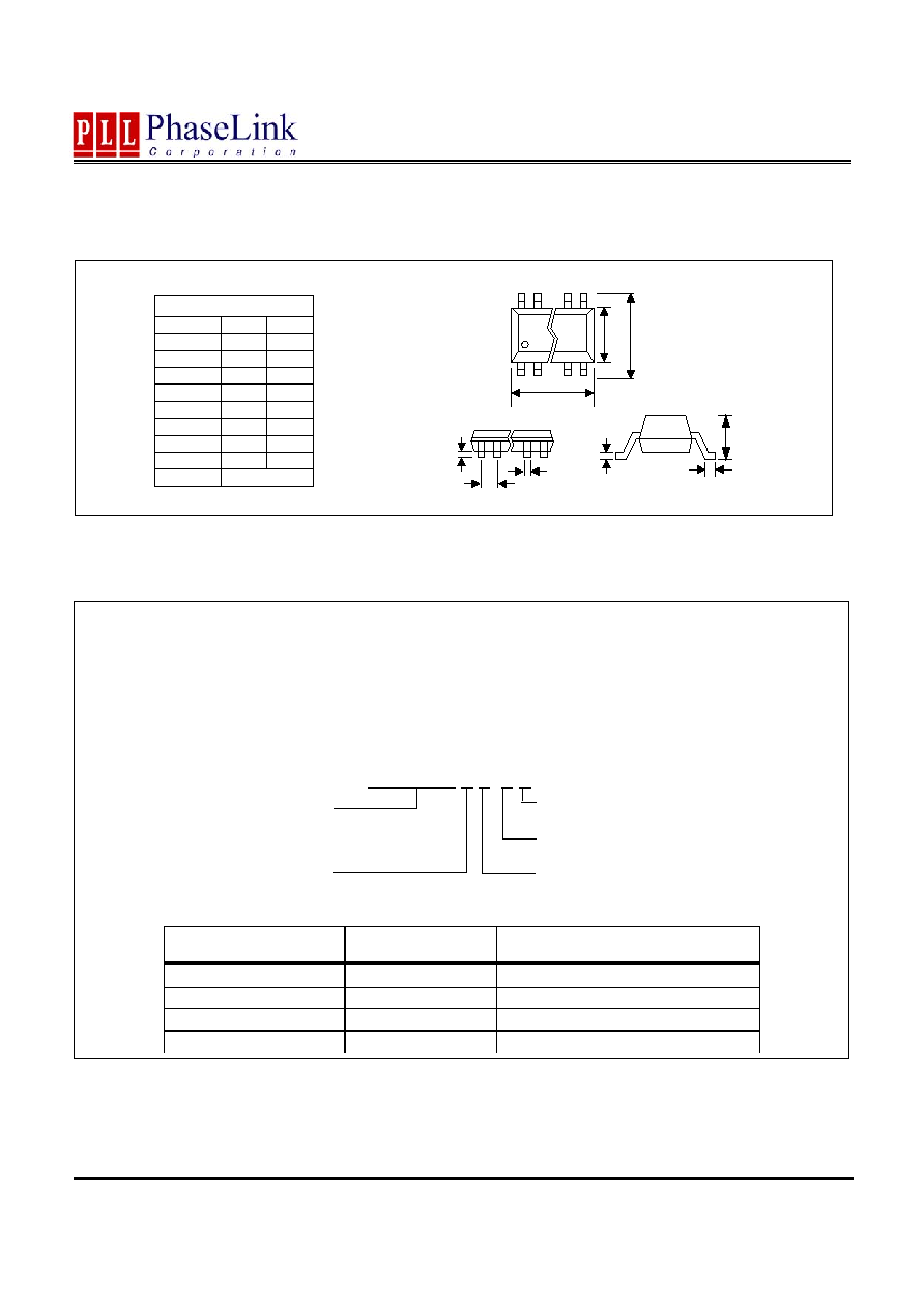
PACKAGE DRAWINGS (GREEN PACKAGE COMPLIANT)
ORDERING INFORMATION
PhaseLink Corporation, reserves the right to make changes in its products or specifications, or both at any time without notice. The information
furnished by Phaselink is believed to be accurate and reliable. However, PhaseLink makes no guarantee or warranty concerning the accuracy of said
information and shall not be responsible for any loss or damage of whatever nature resulting from the use of, or reliance upon this product.
LIFE SUPPORT POLICY: PhaseLink's products are not authorized for use as critical components in life support devices or systems without the
express written approval of the President of PhaseLink Corporation.
For part ordering, please contact our Sales Department:
47745 Fremont Blvd., Fremont, CA 94538, USA
Tel: (510) 492-0990 Fax: (510) 492-0991
PART NUMBER
The order number for this device is a combination of the following:
Device number, Package type and Operating temperature range
PLL601-26 X X X-R
Part / Order Number
Marking
Package Option
PLL601-26SC
P601-26SC
8-Pin SOIC (Tube)
PLL601-26SC-R
P601-26SC
8-Pin SOIC (Tape and Reel)
PLL601-26SCL
P601-26SCL
8-Pin SOIC (Tube), GREEN
PLL601-26SCL-R
P601-26SCL
8-Pin SOIC (Tape and Reel), GREEN
PART NUMBER
TEMPERATURE
C=COMMERCIAL,
I=INDUSTRIAL
PACKAGE TYPE
S=SOIC
NONE=NORMAL PACKAGE
L=GREEN PACKAGE
NONE= TUBE
R=TAPE AND REEL
C
L
A
E
H
D
A1
e
B
8 PIN SOIC (in mm)
Symbol
Min.
Max.
A
1.47
1.73
A1
0.10
0.25
B
0.33
0.51
C
0.19
0.25
D
4.80
4.95
E
3.80
4.00
H
5.80
6.20
L
0.38
1.27
e
1.27 BSC