Preliminary
PLL602-10
96MHz ≠ 400MHz Low Phase Noise XO (for 12 ≠ 25MHz Crystals)
47745 Fremont Blvd., Fremont, California 94538 TEL (510) 492-0990 FAX (510) 492-0991 Rev 11/06/02 Page 1
FEATURES
∑
Low phase noise output for the 96MHz to
400MHz range (-134 dBc at 10kHz offset).
∑
Selectable CMOS, PECL and LVDS output.
∑
12 to 25MHz crystal input.
∑
Output Enable selector.
∑
3.3V operation.
∑
Available in DIE (65 mil x 62 mil).
DESCRIPTIONS
The PLL602-10 is a monolithic low jitter and low
phase noise (-134dBc/Hz @ 10kHz offset) XO IC
Die, with CMOS, LVDS and PECL output, for 96MHz
to 400MHz output range, using a low frequency
crystal.
The same die can be used as a XO with output
frequencies ranging from F
XIN
x 8 to F
XIN
x 16 thanks
to selector pads allowing bonding options (see
Divider Selection Table on this page). This makes
the PLL602-10 ideal for a wide range of applications.
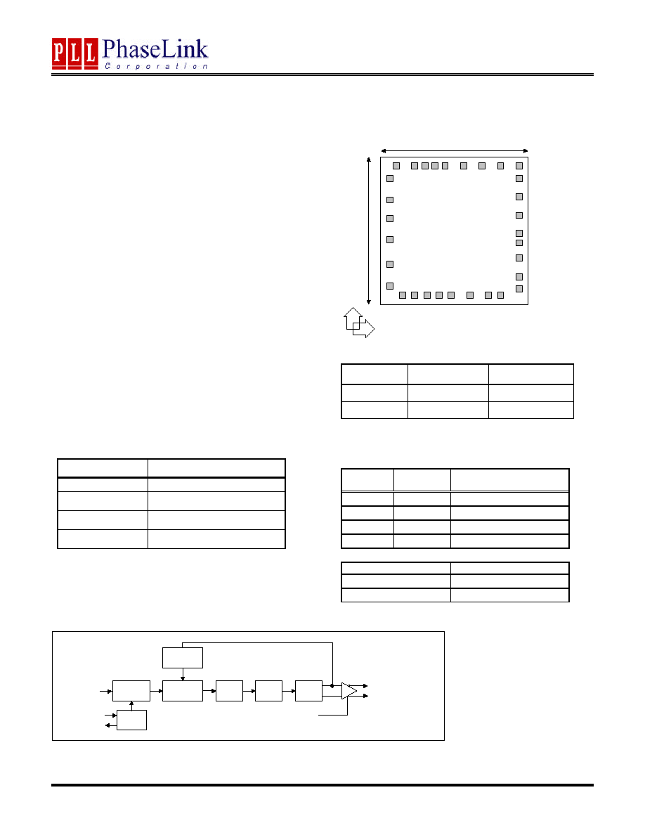
DIE SPECIFICATIONS
Name
Value
Size
62 x 65 mil
Reverse side
GND
Pad dimensions
80 micron x 80 micron
Thickness
10 mil
DIE CONFIGURATION
MULTIPLIER SELECTION
Pad #19
MULTIPLIER
OUTPUT RANGE
0
F
XIN
x 16
192 ≠ 400 MHz
1
F
XIN
x 8
96 ≠ 200 MHz
Note:
Selector pad defaults to `1', wire bond to GND to set to `0'
OUTPUT SELECTION AND ENABLE
Pad #18
OUTSEL1
Pad #25
OUTSEL0
Selected Output
0
0
High Drive CMOS
0
1
Standard CMOS
1
0
PECL
1
1
LVDS
OE (Pad #30)
State
0
Tri-state
1 (Default)
Output enabled
BLOCK DIAGRAM
Reference
Divider
Phase
Comparator
Charge
Pump
Loop
Filter
VCO
VCO
Divider
XTAL
OSC
CLKBAR
OE
XIN
XOUT
CLK
SELECT
18
19
20
21
23
25
7
13
10
26
29
31
Y
X
(0,0)
(1550,1475)
62 mil
65 mil
24
22
17
16
15
14
12
11
9
8
6
1
2
3
4
5
27
28
30

Preliminary
PLL602-10
96MHz ≠ 400MHz Low Phase Noise XO (for 12 ≠ 25MHz Crystals)
47745 Fremont Blvd., Fremont, California 94538 TEL (510) 492-0990 FAX (510) 492-0991 Rev 11/06/02 Page 2
ELECTRICAL SPECIFICATIONS
1. Absolute Maximum Ratings
PARAMETERS
SYMBOL
MIN.
MAX.
UNITS
Supply Voltage
V
DD
7
V
Input Voltage, dc
V
I
V
SS
-
0.5
V
DD
+
0.5
V
Output Voltage, dc
V
O
V
SS
-
0.5
V
DD
+
0.5
V
Storage Temperature
T
S
-65
150
∞
C
Ambient Operating Temperature
T
A
0
70
∞
C
Junction Temperature
T
J
125
∞
C
Lead Temperature (soldering, 10s)
260
∞
C
Input Static Discharge Voltage Protection
2
kV
Exposure of the device under conditions beyond the limits specified by Maximum Ratings for extended periods may cause permanent damage to the
device and affect product reliability. These conditions represent a stress rating only, and functional operations of the device at these or any other
conditions above the operational limits noted in this specification is not implied.
2. Crystal Specifications
PARAMETERS
SYMBOL
CONDITIONS
MIN.
TYP.
MAX.
UNITS
Crystal Resonator
Frequency
F
XIN
Parallel Fundamental
Mode
12
25
MHz
Crystal Loading Rating
C
L
(xtal)
TBD
pF
Recommended ESR
R
E
AT cut
30

Preliminary
PLL602-10
96MHz ≠ 400MHz Low Phase Noise XO (for 12 ≠ 25MHz Crystals)
47745 Fremont Blvd., Fremont, California 94538 TEL (510) 492-0990 FAX (510) 492-0991 Rev 11/06/02 Page 3
3. General Electrical Specifications
PARAMETERS
SYMBOL
CONDITIONS
MIN.
TYP.
MAX.
UNITS
Supply Current, Dynamic
(with Loaded Outputs)
I
DD
PECL/LVDS/CMOS
80/60/35
mA
Operating Voltage
V
DD
3.13
3.47
V
Output Clock Duty Cycle
@ 1.4V (CMOS)
@ 1.25V (LVDS)
@ Vdd ≠ 1.3V (PECL)
45
45
45
50
50
50
55
55
55
%
Short Circuit Current
±
50
mA
4. Jitter and Phase Noise specification
PARAMETERS
CONDITIONS
MIN.
TYP.
MAX.
UNITS
Period jitter RMS
With capacitive decoupling
between VDD and GND.
7
ps
Accumulated jitter RMS
With capacitive decoupling
between VDD and GND. Over
10,000 cycles.
11
ps
Phase Noise relative to carrier
155MHz @100Hz offset
-90
dBc/Hz
Phase Noise relative to carrier
155MHz @1kHz offset
-114
dBc/Hz
Phase Noise relative to carrier
155MHz @10kHz offset
-134
dBc/Hz
Phase Noise relative to carrier
155MHz @100kHz offset
-134
dBc/Hz

Preliminary
PLL602-10
96MHz ≠ 400MHz Low Phase Noise XO (for 12 ≠ 25MHz Crystals)
47745 Fremont Blvd., Fremont, California 94538 TEL (510) 492-0990 FAX (510) 492-0991 Rev 11/06/02 Page 4
5. LVDS Electrical Characteristics
PARAMETERS
SYMBOL
CONDITIONS
MIN.
TYP.
MAX.
UNITS
Output Differential Voltage
V
OD
247
355
454
mV
V
DD
Magnitude Change
V
OD
-50
50
mV
Output High Voltage
V
OH
1.4
1.6
V
Output Low Voltage
V
OL
0.9
1.1
V
Offset Voltage
V
OS
1.125
1.2
1.375
V
Offset Magnitude Change
V
OS
R
L
= 100
(see figure)
0
3
25
mV
Power-off Leakage
I
OXD
V
out
= V
DD
or GND
V
DD
= 0V
±
1
±
10
uA
Output Short Circuit Current
I
OSD
-5.7
-8
mA
6. LVDS Switching Characteristics
PARAMETERS
SYMBOL
CONDITIONS
MIN.
TYP.
MAX.
UNITS
Differential Clock Rise Time
t
r
0.2
0.7
1.0
ns
Differential Clock Fall Time
t
f
R
L
= 100
C
L
= 10 pF
(see figure)
0.2
0.7
1.0
ns
OUT
OUT
V
OD
V
OS
50
50
OUT
V
DIFF
R
L
= 100
C
L
= 10pF
C
L
= 10pF
LVDS Switching Test Circuit
LVDS Levels Test Circuit
LVDS Transistion Time Waveform
OUT
OUT
OUT
0V (Differential)
0V
20%
80%
20%
80%
t
R
t
F
V
DIFF

Preliminary
PLL602-10
96MHz ≠ 400MHz Low Phase Noise XO (for 12 ≠ 25MHz Crystals)
47745 Fremont Blvd., Fremont, California 94538 TEL (510) 492-0990 FAX (510) 492-0991 Rev 11/06/02 Page 5
7. PECL Electrical Characteristics
PARAMETERS
SYMBOL
CONDITIONS
MIN.
MAX.
UNITS
Output High Voltage
V
OH
V
DD
≠ 1.025
V
Output Low Voltage
V
OL
R
L
= 50
to (V
DD
≠ 2V)
(see figure)
V
DD
≠ 1.620
V
8. PECL Switching Characteristics
PARAMETERS
SYMBOL
CONDITIONS
MIN.
TYP.
MAX.
UNITS
Clock Rise Time
t
r
@20/80% - PECL
0.6
1.5
ns
Clock Fall Time
t
f
@80/20% - PECL
0.5
1.5
ns
OUT
OUT
50
50
PECL Levels Test Circuit
PECL Transistion Time Waveform
OUT
OUT
50%
20%
80%
t
R
t
F
VDD
DUTY CYCLE
45 - 55%
55 - 45%
50%
OUT
OUT
t
SKEW
PECL Output Skew
2.0V
Preliminary
PLL602-10
96MHz ≠ 400MHz Low Phase Noise XO (for 12 ≠ 25MHz Crystals)
47745 Fremont Blvd., Fremont, California 94538 TEL (510) 492-0990 FAX (510) 492-0991 Rev 11/06/02 Page 6
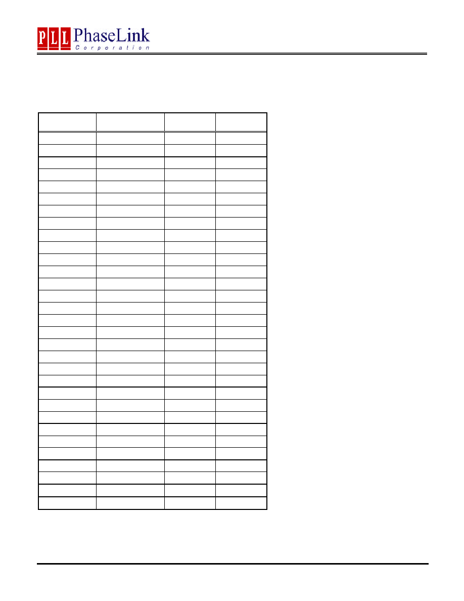
PAD ASSIGNMENT
Pad #
Name
X (
µ
µ
m)
Y (
µ
µ
m)
1
GND
248
109
2
GND
361
109
3
GND
473
109
4
GND
587
109
5
GND
702
109
6
N/C
874
109
7
GND
1042
109
8
GNDBUF
1171
109
9
CMOS
1400
125
10
LVDS
1400
259
11
PECL
1400
476
12
VDDBUF
1400
616
13
VDDBUF
1400
716
14
PECLB
1400
871
15
LVDSB
1400
1089
16
CMOSB
1400
1227
17
GNDBUF
1389
1365
18
OUTSEL1
1232
1365
19
FSEL
1042
1365
20
N/C
854
1365
21
VDD
659
1365
22
VDD
559
1365
23
VDD
459
1365
24
VDD
358
1365
25
OUTSEL0
194
1365
26
XIN
109
1223
27
XOUT
109
1017
28
N/C
109
858
29
N/C
109
646
30
OE
109
397
31
N/C
109
181

Preliminary
PLL602-10
96MHz ≠ 400MHz Low Phase Noise XO (for 12 ≠ 25MHz Crystals)
47745 Fremont Blvd., Fremont, California 94538 TEL (510) 492-0990 FAX (510) 492-0991 Rev 11/06/02 Page 7
ORDERING INFORMATION
PhaseLink Corporation, reserves the right to make changes in its products or specifications, or both at any time without notice. The information
furnished by Phaselink is believed to be accurate and reliable. However, PhaseLink makes no guarantee or warranty concerning the accuracy of said
information and shall not be responsible for any loss or damage of whatever nature resulting from the use of, or reliance upon this product.
LIFE SUPPORT POLICY: PhaseLink's products are not authorized for use as critical components in life support devices or systems without the
express written approval of the President of PhaseLink Corporation.
For part ordering, please contact our Sales Department:
47745 Fremont Blvd., Fremont, CA 94538, USA
Tel: (510) 492-0990 Fax: (510) 492-0991
PART NUMBER
The order number for this device is a combination of the following:
Device number, Package type and Operating temperature range
PLL602-10 D C
PART NUMBER
TEMPERATURATRE
C=COMMERCIAL
M=MILITARY
I=INDUSTRAL
PACKAGE TYPE
D=DIE