
PLL602-20
200MHz XO IC With Selectable 4X/8X Multiplier
47745 Fremont Blvd., Fremont, California 94538 Tel (510) 492-0990 Fax (510) 492-0991 www.phaselink.com Rev 02/18/05 Page 1
FEATURES
∑ Integrated crystal oscillator circuitry (XO).
∑ Very low Jitter and Phase Noise (-110dBc @
10kHz offset)
∑ Selectable frequency multiplication (x4, x8).
∑ Accepts Fundamental Crystal input of 10MHz-30MHz
∑ Output Frequency: up to 200MHz CMOS
∑ Output enable (OE) pin with 60K pull up
resistor
∑ Operating temperature range from 0įC to 70įC
∑ 2.5 or 3.3V supply voltage.
∑ Available in Green/RoHS compliant 8-pin SOIC
package
DESCRIPTION
The PLL602-20 is a general purpose low jitter and
low phase noise (-110dBc @10kHz offset), high
performance CMOS XO IC. This flexible device can
be used as a XO with output frequencies ranging
from F
XIN
x 4 to F
XIN
x 8 with the use of a single
selector pin. This makes the PLL602-20 the ideal
high performance, low-cost solution for a wide range
of applications requiring up to 200MHz (including
77.76MHz, 125MHz and 155.52MHz).
BLOCK DIAGRAM
PIN CONFIGURATION
PAD LAYOUT AND DIE ID
DIE SPECIFICATION
Name Value
Size 31.5x55.1
mil
Reverse side
GND
Pad Opening
80 micron x 80 micron
Die Thickness
10 mil
XIn
XO
CLK
Selectable
PLL
XOut
SELx4x/8
1
2
3
4
5
6
7
8
XIN/FIN
GND
SEL
4
X
/
8
X
CLK
XOUT
NC
VDD
OE
PLL602
-20
XIN
GND
GND
SEL4X/8X
1
2
3
4
5
9
6
7
8
XOUT
OE
VDD
VDD
1
2
3
4
5
9
6
7
8
CLK
C

PLL602-20
200MHz XO IC With Selectable 4X/8X Multiplier
47745 Fremont Blvd., Fremont, California 94538 Tel (510) 492-0990 Fax (510) 492-0991 www.phaselink.com Rev 02/18/05 Page 2
PIN/PAD ASSIGNMENT and DESCRIPTION
Die Pads
Name Pin
#
Pad #
X (Ķm)
Y(Ķm)
Type Description
XIN/FIN
1
1
101.5
1274.0
I
Crystal or Reference Input Pin.
2
101.5
1075.0
GND
2 3 101.5
878.4
P GND
connection.
SEL4X/8X 3 4 101.5 671.8 O
Multiplier Selector Pin with 60K pull-up resistor.
Logic State
Multiplier
0 x4
1(default) x8
CLK 4 5
101.5
425.0
O
Clock
Output.
6
697
483.0
VDD 5
7 697
790.0
P VDD
connection.
DNC
6
-
-
-
-
Do Not Connect.
OE 7
8
697
1024.0
O
Output Enable: `0' to disable (tri-state output), 1'
(default value when not connected) to enable the
output (internal (60K pull up resistor).
XOUT 8 9 697
1274.0
O
Crystal
output.
PLL602-20
200MHz XO IC With Selectable 4X/8X Multiplier
47745 Fremont Blvd., Fremont, California 94538 Tel (510) 492-0990 Fax (510) 492-0991 www.phaselink.com Rev 02/18/05 Page 3
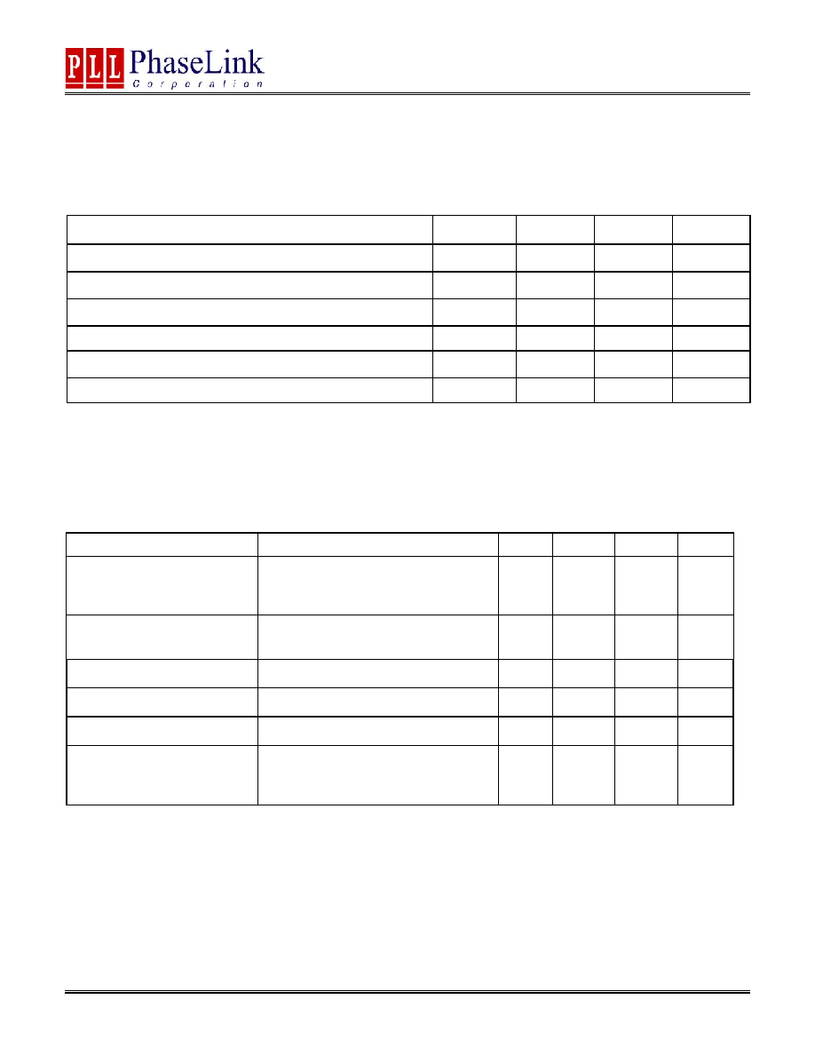
ELECTRICAL SPECIFICATIONS
ABSOLUTE MAXIMUM RATINGS
PARAMETERS SYMBOL
MIN.
MAX.
UNITS
Supply Voltage Range
V
DD
-
0.5
4.6 V
Input Voltage Range
V
I
-
0.5 V
DD
+
0.5
V
Output Voltage Range
V
O
-
0.5 V
DD
+
0.5
V
Soldering Temperature (Green package)
260
įC
Storage Temperature
T
S
-65 150
įC
Ambient Operating Temperature
0
70
įC
Exposure of the device under conditions beyond the limits specified by Maximum Ratings for extended periods may cause permanent damage to the
device and affect product reliability. These conditions represent a stress rating only, and functional operations of the device at these or any other
conditions above the operational limits noted in this specification is not implied.
AC SPECIFICATIONS
PARAMETERS CONDITIONS
MIN.
TYP.
MAX.
UNITS
Crystal Input Frequency(XIN)
Fundamental Crystal
10
30
MHz
Settling Time
At power-up (after VDD increases over
1.62V)
10
ms
Output Rise Time
15pF Load, 10/90%VDD
1.2
2.0
ns
Output Fall Time
15pF Load, 90/10%VDD
1.2
2.0
ns
Duty Cycle
At VDD/2
45
50
55
%
Period Jitter, peak-to-peak*
(measured from 10,000
samples)
With capacitive decoupling between VDD
and GND. Operating only one output.
70
ps

PLL602-20
200MHz XO IC With Selectable 4X/8X Multiplier
47745 Fremont Blvd., Fremont, California 94538 Tel (510) 492-0990 Fax (510) 492-0991 www.phaselink.com Rev 02/18/05 Page 4
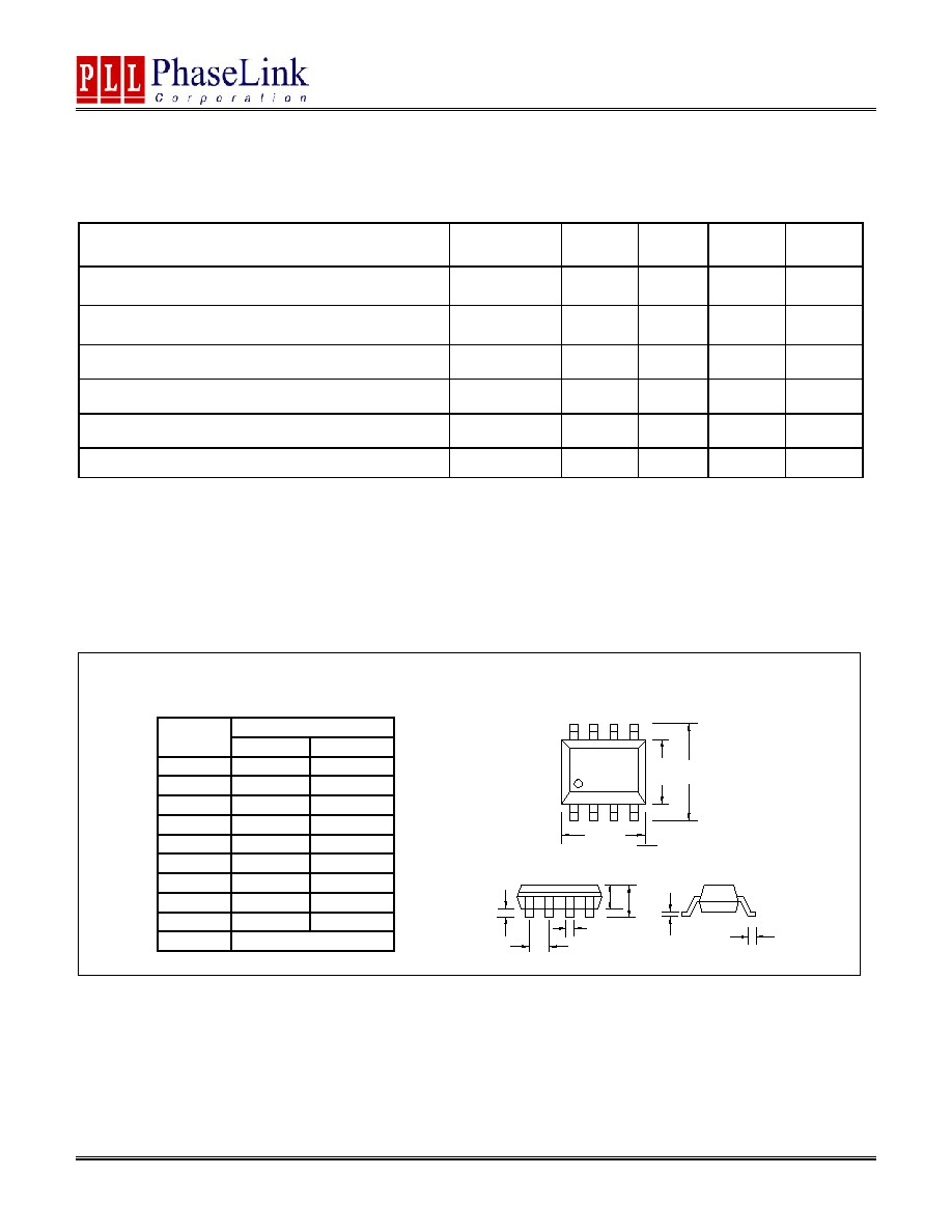
DC SPECIFICATIONS
PARAMETERS SYMBOL
CONDITIONS MIN.
TYP.
MAX.
UNITS
Supply Current, Dynamic, with
Loaded Outputs
I
DD
At 80MHz, load=15pF,
VDD=3.3V
15
mA
Operating Voltage
V
DD
2.25
3.63
V
Output Low Voltage
V
OL
I
OL
= +4mA Std. drive
0.4
V
Output High Voltage
V
OH
I
OH
= -4mA Std. drive
V
DD
≠ 0.4
V
Output Current
I
OSD
V
OL
= 0.4V, V
OH
= 2.4V
24
mA
Short-circuit Current
I
S
Ī50
mA
JITTER AND PHASE NOISE SPECIFICATION
PARAMETERS CONDITIONS
MIN.
TYP.
MAX.
UNITS
at 155MHz, with capacitive decoupling
between VDD and GND.
50
Period Jitter
(PkPk ≠ 10,000 samples)
at 80MHz, with capacitive decoupling
between VDD and GND.
55
ps
Phase Noise relative to carrier
125MHz @100Hz offset
-100
dBc/Hz
Phase Noise relative to carrier
125MHz @1kHz offset
-118
dBc/Hz
Phase Noise relative to carrier
125MHz @10kHz offset
-112
dBc/Hz
Phase Noise relative to carrier
125MHz @100kHz offset
-98
dBc/Hz
Phase Noise relative to carrier
125MHz @1MHz offset
-107
dBc/Hz
PLL602-20
200MHz XO IC With Selectable 4X/8X Multiplier
47745 Fremont Blvd., Fremont, California 94538 Tel (510) 492-0990 Fax (510) 492-0991 www.phaselink.com Rev 02/18/05 Page 5
CRYSTAL SPECIFICATIONS
PARAMETERS SYMBOL
MIN.
TYP.
MAX.
UNITS
Fundamental Crystal Resonator Frequency
F
XIN
10 30
MHz
Crystal Loading Rating
C
L (xtal)
11 pF
Maximum Sustainable Drive Level
500
ĶW
Operating Drive Level
100
ĶW
Crystal Shunt Capacitance
C0
6
pF
Effective Series Resistance, Fundamental, 10-30MHz
R
E
30
Note: A detailed crystal specification document is also available for this part
PACKAGE DRAWINGS (GREEN PACKAGE COMPLIANT)
SOIC 8L
Dimension in MM
Symbol
Min. Max.
A 1.35 1.75
A1 0.10 0.25
A2 1.25 1.50
B 0.33 0.53
C 0.19 0.27
D 4.80 5.00
E 3.80 4.00
H 5.80 6.20
L 0.40 0.89
e 1.27
BSC
C
L
A2
E
H
D
A1
e
b
A

PLL602-20
200MHz XO IC With Selectable 4X/8X Multiplier
47745 Fremont Blvd., Fremont, California 94538 Tel (510) 492-0990 Fax (510) 492-0991 www.phaselink.com Rev 02/18/05 Page 6
ORDERING INFORMATION
PhaseLink Corporation, reserves the right to make changes in its products or specifications, or both at any time without notice. The information
furnished by Phaselink is believed to be accurate and reliable. However, PhaseLink makes no guarantee or warranty concerning the accuracy of said
information and shall not be responsible for any loss or damage of whatever nature resulting from the use of, or reliance upon this product.
LIFE SUPPORT POLICY: PhaseLink's products are not authorized for use as critical components in life support devices or systems without the
express written approval of the President of PhaseLink Corporation.
For part ordering, please contact our Sales Department:
47745 Fremont Blvd., Fremont, CA 94538, USA
Tel: (510) 492-0990 Fax: (510) 492-0991
PART NUMBER
The order number for this device is a combination of the following:
Device number, Package type and Operating temperature range
PLL602-20 X X-R
* PhaseLink Offers Green/RoHS Compliant Packaging Only.
Part / Order
Number
Marking Package
Option
PLL602-20SC
P602-20SC
8-Pin SOIC (Tube)
PLL602-20SC-R
P602-20SC
8-Pin SOIC (Tape & Reel)
PART NUMBER
TEMPERATURE
C=COMMERCIAL
I = INDUSTRIAL
PACKAGE TYPE*
S=SOIC
NONE= TUBE
R=TAPE and REEL