PLL602-35/-37/-38/-39
750kHz ≠ 800MHz Low Phase Noise Multiplier XO
Universal Low Phase Noise IC's
47745 Fremont Blvd., Fremont, California 94538 Tel (510) 492-0990 Fax (510) 492-0991 www.phaselink.com Rev 11/28/05 Page 1
FEATURES
∑ Selectable 750kHz to 800MHz range.
∑ Low phase noise output (@ 10kHz frequency
offset, -140dBc/Hz for 19.44MHz, -127dBc/Hz for
106.25MHz, -125dBc/Hz for 155.52MHz, -
110dBc/Hz for 622.08MHz).
∑ CMOS (PLL602-37), PECL (PLL602-35 and
PLL602-38) or LVDS (PLL602-39) output.
∑ 12 to 25MHz crystal input.
∑ No external load capacitor required.
∑ Output Enable selector.
∑ Selectable 1/16 to 32x frequency multiplier.
∑ 3.3V operation.
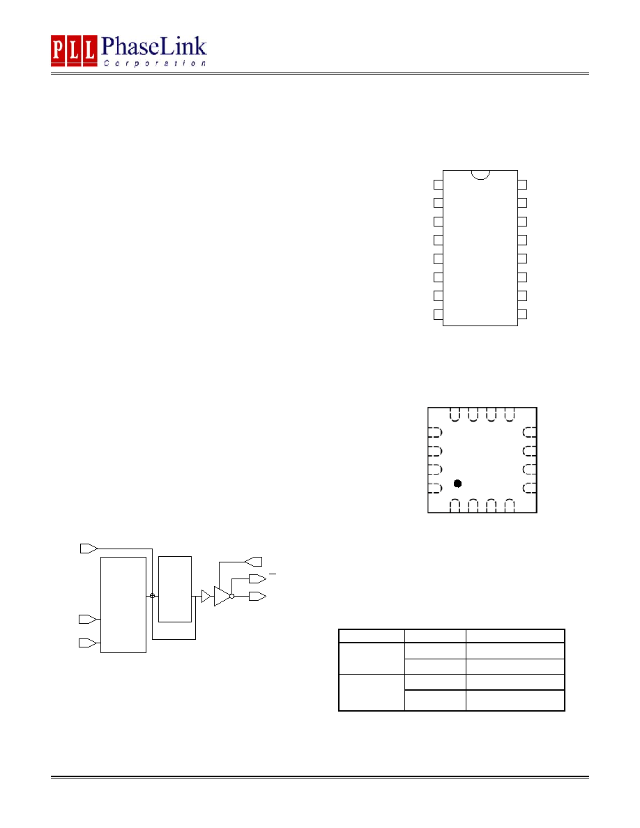
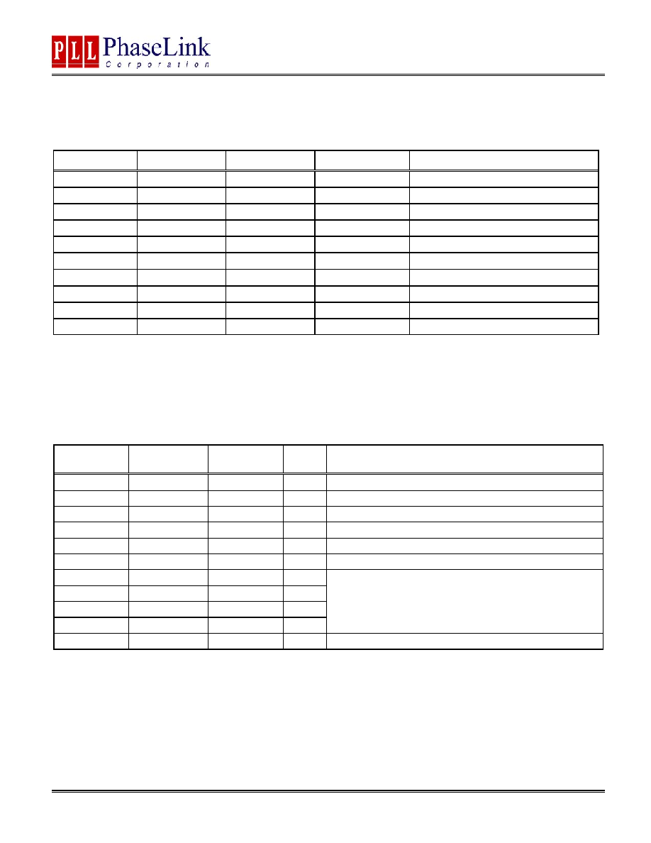
∑ Available in 16-Pin (TSSOP or 3x3mm QFN).
DESCRIPTION
The PLL602-35 (PECL with inverted OE), PLL602-37
(CMOS), PLL602-38 (PECL), and PLL602-39 (LVDS)
are high performance and low phase noise XO IC
chips. They provide phase noise performance as low
as ≠125dBc at 1kHz offset (at 155MHz) and a typical
RMS jitter of 4pS RMS ( at 155MHz ). They accept
fundamental parallel resonant mode crystals from 12
to 25MHz.
BLOCK DIAGRAM
PIN CONFIGURATION
(Top View)
^: Internal
pull-up
*: On 3x3 package, PLL602-35/-38 do not have SEL0 available: Pin
10 is VDD, pin 11 is GND. However, PLL602-37/-39 have SEL0
(pin 10), and pin 11 is VDD. See pin assignment table for details.
OUTPUT ENABLE LOGICAL LEVELS
Part #
OE
State
0 (Default) Output enabled
PLL602-38
1 Tri-state
0 Tri-state
PLL602-35
PLL602-37
PLL602-39
1 (Default) Output enabled
OE input: Logical states defined by PECL levels for PLL602-38
Logical states defined by CMOS levels for
PLL602-35/-37/-39
PLL 602-3X
1
2
3
4
5
6
7
8
VDD
9
10
11
12
13
14
15
16
XIN
XOUT
SEL3^
SEL2^
OE
GND
GND
SEL0^
SEL1^
GND
CLKC
VDD
CLKT
GND
GND
PLL602-3X
GND
VDD
CLKT
CLKC
1
2
3
4
12
11
10
9
13
14
15
16
8
7
6
5
XIN
SE
L0
^ /
V
D
D*
SEL1^
VD
D /
G
ND*
SEL3^
XOUT
SEL2^
OE
GN
D
GN
D
GN
D
GN
D
XIN
XOUT
OE
Q
PLL602-3x
Q
PLL by-pass
SEL
PLL
(Phase
Locked
Loop)
Oscillator
Amplifier
PLL602-35/-37/-38/-39
750kHz ≠ 800MHz Low Phase Noise Multiplier XO
Universal Low Phase Noise IC's
47745 Fremont Blvd., Fremont, California 94538 Tel (510) 492-0990 Fax (510) 492-0991 www.phaselink.com Rev 11/28/05 Page 2
FREQUENCY SELECTION TABLE
SEL3
SEL2 SEL1 SEL0
Selected
Multiplier
0
0
1
1
Fin x 32
0 1 1 0
Fin
/
8
0
1
1
1
Fin x 2
1 0 0 1
Fin
/
2
1 0 1 0
Fin
/
16
1
0
1
1
Fin x 4
1 1 0 0
Fin
/
4
1
1
0
1
Fin x 8
1
1
1
0
Fin x 16
1 1 1 1
No
multiplication
Note: SEL0 is not available (always "1") for PLL602-35 and PLL602-38 in 3x3mm package
PIN DESCRIPTIONS PLL602-35 and PLL602-38 (see next page of PLL602-37/-39)
Name
TSSOP
Pin number
3x3mm QFN
Pin number
Type Description
XIN
2
12
I
Crystal input. See Crystal Specifications on page 3.
XOUT
3
13
I
Crystal output. See Crystal Specifications on page 3.
OE
6
16
I
Output enable pin (see OE logic state table on page 1).
GND 7,8,9,10,14
1,2,3,4,8,11
P
Ground.
CLKT 11 5
O
True
output
PECL
CLKC 13 7 O
Complementary
output
PECL.
SEL0 16
Not
available
I
SEL1 15 9 I
SEL2 5 15
I
SEL3 4 14
I
Multiplier selector pins. These pins have an internal pull-up
that will default SEL to `1' when not connected to GND.
VDD 1,
12 6,10
P
Power
Supply.
PLL602-35/-37/-38/-39
750kHz ≠ 800MHz Low Phase Noise Multiplier XO
Universal Low Phase Noise IC's
47745 Fremont Blvd., Fremont, California 94538 Tel (510) 492-0990 Fax (510) 492-0991 www.phaselink.com Rev 11/28/05 Page 3
PIN DESCRIPTIONS PLL602-37/-39 (see previous page of PLL602-35/-38)
Name
TSSOP
Pin number
3x3mm QFN
Pin number
Type Description
XIN
2
12
I
Crystal input. See Crystal Specifications on page 3.
XOUT
3
13
I
Crystal output. See Crystal Specifications on page 3.
OE
6
16
I
Output enable pin (see OE logic state table on page 1).
GND 7,8,9,10,14
1,2,3,4,8 P
Ground.
CLKT 11 5
O
True output LVDS (PLL602-39)
(N/C for PLL602-37)
CLKC 13 7 O
Complementary output LVDS (PLL602-39)
(CMOS out for PLL602-37).
SEL0 16 10
I
SEL1 15 9 I
SEL2 5 15
I
SEL3 4 14
I
Multiplier selector pins. These pins have an internal pull-up
that will default SEL to `1' when not connected to GND.
VDD 1,
12 6,11
P
Power
Supply.
ELECTRICAL SPECIFICATIONS
1. Absolute Maximum Ratings
PARAMETERS SYMBOL
MIN.
MAX.
UNITS
Supply Voltage
V
DD
4.6 V
Input Voltage, dc
V
I
-0.5
V
DD
+0.5 V
Output Voltage, dc
V
O
-0.5
V
DD
+0.5 V
Storage Temperature
T
S
-65 150
∞C
Ambient Operating Temperature*
T
A
-40 85
∞C
Junction Temperature
T
J
125
∞C
Lead Temperature (soldering, 10s)
260
∞C
ESD Protection, Human Body Model
2
kV
Exposure of the device under conditions beyond the limits specified by Maximum Ratings for extended periods may cause permanent damage to the
device and affect product reliability. These conditions represent a stress rating only, and functional operations of the device at these or any other con-
ditions above the operational limits noted in this specification is not implied.
* Note: Operating Temperature is guaranteed by design for all parts (COMMERCIAL and INDUSTRIAL), but tested for COMMERCIAL grade only.
2. Crystal Specifications
PARAMETERS SYMBOL CONDITIONS MIN.
TYP.
MAX.
UNITS
Crystal Resonator Frequency
F
XIN
Parallel Fundamental Mode
12
25
MHz
Crystal Loading Rating
C
L (xtal)
20
pF
Recommended ESR
R
E
AT cut
30
PLL602-35/-37/-38/-39
750kHz ≠ 800MHz Low Phase Noise Multiplier XO
Universal Low Phase Noise IC's
47745 Fremont Blvd., Fremont, California 94538 Tel (510) 492-0990 Fax (510) 492-0991 www.phaselink.com Rev 11/28/05 Page 4
3. General Electrical Specifications
PARAMETERS SYMBOL
CONDITIONS
MIN. TYP. MAX. UNITS
Fout<24MHz
25/25/15
24MHz<Fout<96MHz
65/45/30
Supply Current,
Dynamic (with
Loaded Outputs)
I
DD
PECL/LVDS/CMOS
96MHz<Fout<800MHz
100/80/40
mA
Operating Voltage
V
DD
2.97
3.63 V
Output Clock
Duty Cycle
@ 50% V
DD
(CMOS)
@ 1.25V (LVDS)
@
V
DD
≠ 1.3V (PECL)
45
45
45
50
50
50
55
55
55
%
Short Circuit
Current
±50
mA
4. Jitter Specifications
PARAMETERS CONDITIONS
FREQUENCY MIN. TYP. MAX. UNITS
19.44MHz 2.2
77.76MHz 3.5
155.52MHz 4.3
Period jitter RMS
1
With capacitive decoupling be-
tween VDD and GND.
Over 10,000 cycles.
622.08MHz 5.0
ps
19.44MHz 17
77.76MHz 25
155.52MHz 27
Period jitter Peak-to-
Peak
1
With capacitive decoupling be-
tween VDD and GND.
Over 10,000 cycles.
622.08MHz 35
ps
155.52MHz 2.6 4
Integrated jitter RMS
2
Integrated 12 kHz to 20 MHz
622.08MHz 2.5 4
ps
5. Phase Noise Specifications
PARAMETERS FREQUENCY @10Hz
@100Hz @1kHz @10kHz @100kHz UNITS
19.44MHz -80 -108
-132
-142
-150
77.76MHz -72 -103
-122
-130
-125
155.52MHz -65 -95
-120
-125
-121
Phase Noise
2
relative
to carrier
(typical)
622.08MHz -55 -85
-109
-115
-110
dBc/Hz
6. CMOS Electrical Characteristics
PARAMETERS SYMBOL CONDITIONS MIN.
TYP.
MAX.
UNITS
I
OH
V
OH
= V
DD
-0.4V, V
DD
=3.3V 10 mA
Output drive current
I
OL
V
OL
= 0.4V, V
DD
= 3.3V
10
mA
Output Clock Rise/Fall Time
0.3V ~ 3.0V with 15 pF load
2.4
ns
PLL602-35/-37/-38/-39
750kHz ≠ 800MHz Low Phase Noise Multiplier XO
Universal Low Phase Noise IC's
47745 Fremont Blvd., Fremont, California 94538 Tel (510) 492-0990 Fax (510) 492-0991 www.phaselink.com Rev 11/28/05 Page 5
7. LVDS Electrical Characteristics
PARAMETERS SYMBOL
CONDITIONS
MIN.
TYP.
MAX.
UNITS
Output Differential Voltage
V
OD
247
355
454
mV
V
DD
Magnitude Change
V
OD
-50 50 mV
Output High Voltage
V
OH
1.4
1.6
V
Output Low Voltage
V
OL
0.9
1.1
V
Offset Voltage
V
OS
1.125
1.2
1.375
V
Offset Magnitude Change
V
OS
R
L
= 100
(see figure)
0 3 25 mV
Power-off Leakage
I
OXD
V
out
= V
DD
or GND
V
DD
= 0V
±1
±10
uA
Output Short Circuit Current
I
OSD
-5.7 -8
mA
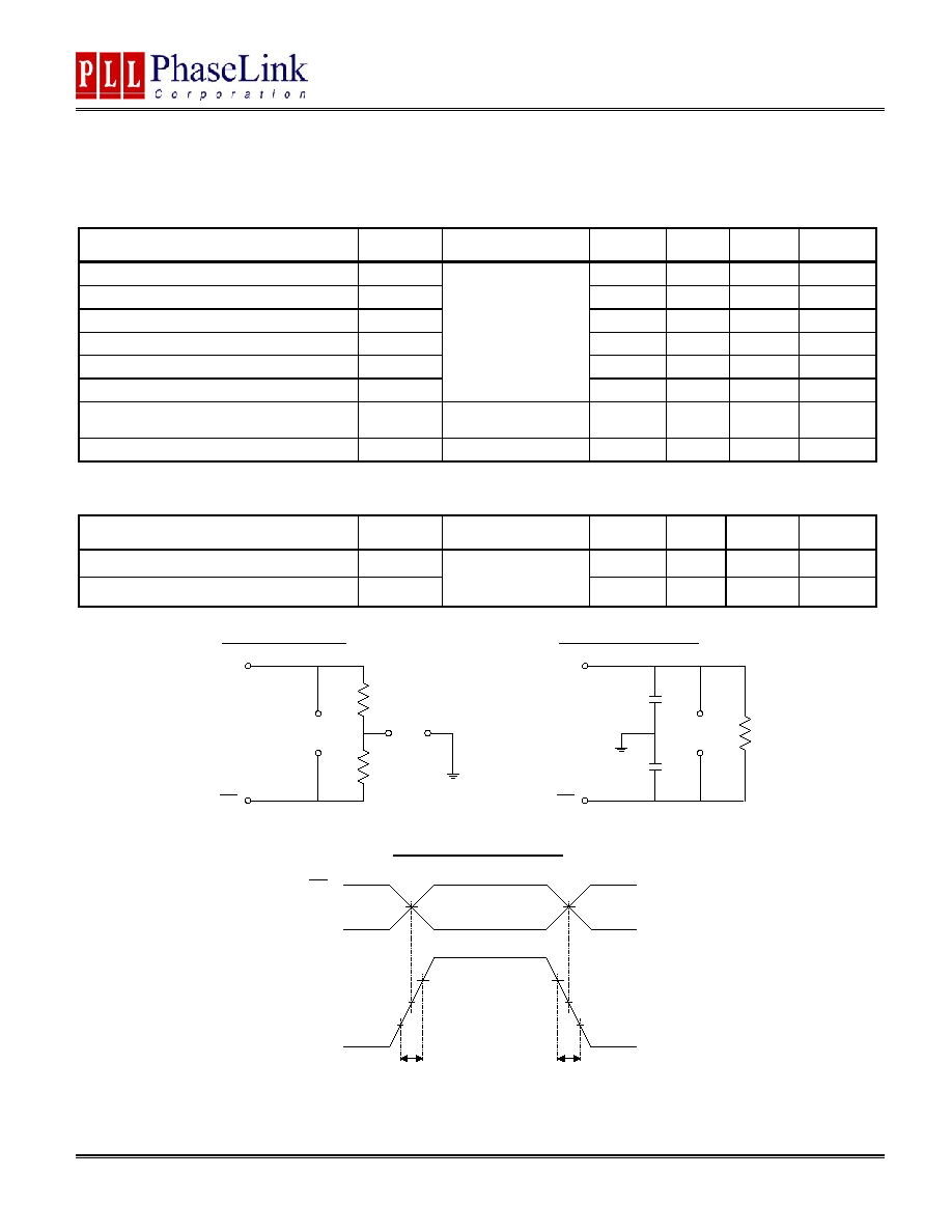
8. LVDS Switching Characteristics
PARAMETERS SYMBOL
CONDITIONS
MIN.
TYP.
MAX.
UNITS
Differential Clock Rise Time
t
r
0.2 0.7 1.0 ns
Differential Clock Fall Time
t
f
R
L
= 100
C
L
= 10 pF
(see figure)
0.2 0.7 1.0 ns
OUT
OUT
V
OD
V
OS
50
50
OUT
V
DIFF
R
L
= 100
C
L
= 10pF
C
L
= 10pF
LVDS Switching Test Circuit
LVDS Levels Test Circuit
LVDS Transistion Time Waveform
OUT
OUT
OUT
0V (Differential)
0V
20%
80%
20%
80%
t
R
t
F
V
DIFF

PLL602-35/-37/-38/-39
750kHz ≠ 800MHz Low Phase Noise Multiplier XO
Universal Low Phase Noise IC's
47745 Fremont Blvd., Fremont, California 94538 Tel (510) 492-0990 Fax (510) 492-0991 www.phaselink.com Rev 11/28/05 Page 6
9. PECL Electrical Characteristics
PARAMETERS SYMBOL CONDITIONS
MIN. MAX.
UNITS
Output High Voltage
V
OH
V
DD
≠ 1.025
V
Output Low Voltage
V
OL
R
L
= 50
to (V
DD
≠ 2V)
(see figure)
V
DD
≠ 1.620
V
10. PECL Switching Characteristics
PARAMETERS SYMBOL CONDITIONS MIN.
TYP.
MAX.
UNITS
Clock Rise Time
t
r
0.8V ~ 2.0V
1.5
ns
Clock Fall Time
t
f
2.0V ~ 0.8V
1.5
ns
Duty Cycle
Measured @ 1.4V
40
50
60
%
OUT
OUT
50
50
PECL Levels Test Circuit
PECL Transistion Time Waveform
OUT
OUT
50%
20%
80%
t
R
t
F
VDD
DUTY CYCLE
45 - 55%
55 - 45%
50%
OUT
OUT
t
SKEW
PECL Output Skew
2.0V
PLL602-35/-37/-38/-39
750kHz ≠ 800MHz Low Phase Noise Multiplier XO
Universal Low Phase Noise IC's
47745 Fremont Blvd., Fremont, California 94538 Tel (510) 492-0990 Fax (510) 492-0991 www.phaselink.com Rev 11/28/05 Page 7
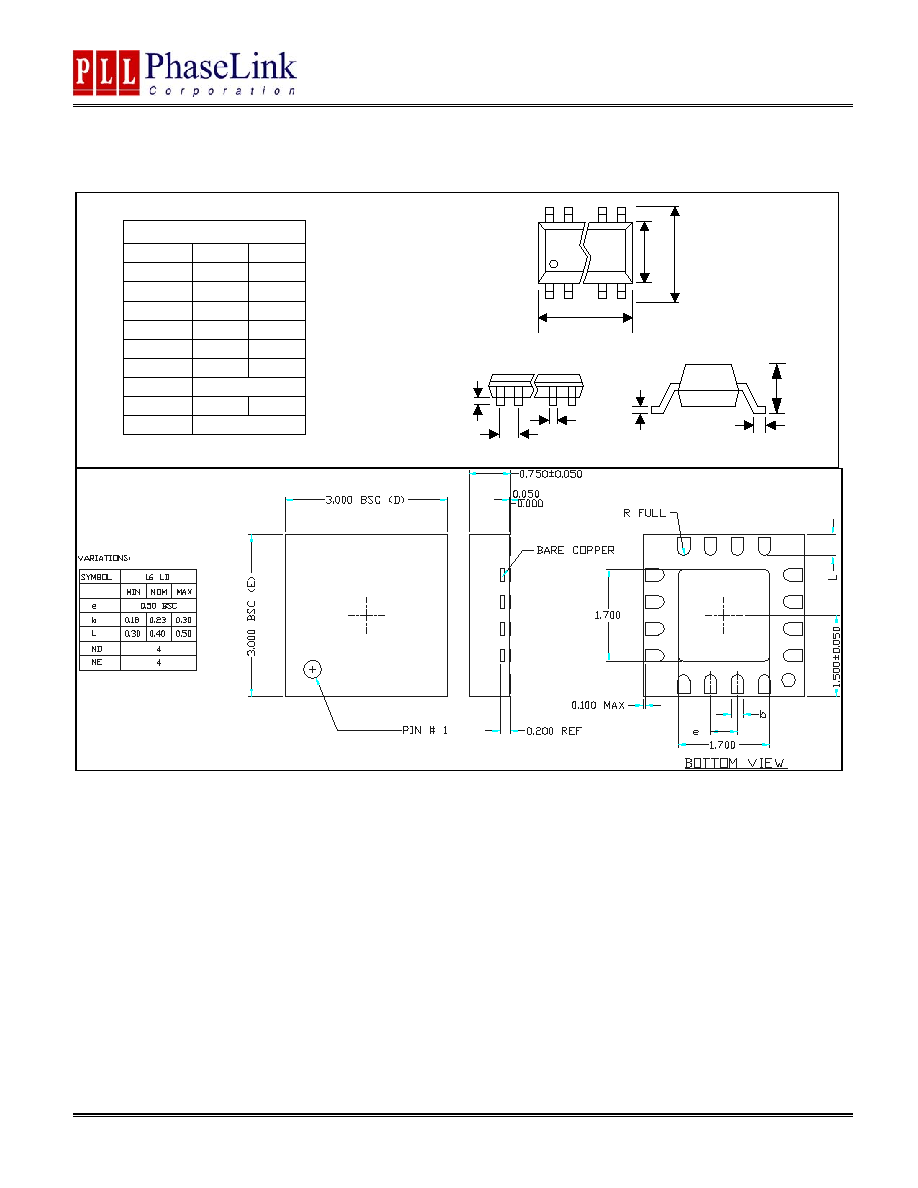
PACKAGE INFORMATION
C
L
A
E
H
D
A1
e
B
16 PIN TSSOP ( mm )
Symbol
Min.
Max.
A
-
1.20
A1
0.05
0.15
B
0.19
0.30
C
0.09
0.20
D
4.90
5.10
E
4.30
4.50
H
6.40 BSC
L
0.45
0.75
e
0.65 BSC
3x3mm QFN
PLL602-35/-37/-38/-39
750kHz ≠ 800MHz Low Phase Noise Multiplier XO
Universal Low Phase Noise IC's
47745 Fremont Blvd., Fremont, California 94538 Tel (510) 492-0990 Fax (510) 492-0991 www.phaselink.com Rev 11/28/05 Page 8
ORDERING INFORMATION
PhaseLink Corporation, reserves the right to make changes in its products or specifications, or both at any time without notice. The information fur-
nished by Phaselink is believed to be accurate and reliable. However, PhaseLink makes no guarantee or warranty concerning the accuracy of said
information and shall not be responsible for any loss or damage of whatever nature resulting from the use of, or reliance upon this product.
LIFE SUPPORT POLICY: PhaseLink's products are not authorized for use as critical components in life support devices or systems without the ex-
press written approval of the President of PhaseLink Corporation.
For part ordering, please contact our Sales Department:
47745 Fremont Blvd., Fremont, CA 94538, USA
Tel: (510) 492-0990 Fax: (510) 492-0991
PART NUMBER
The order number for this device is a combination of the following:
Device number, Package type and Operating temperature range
PLL602-3X X
C
X X
Order Number Marking Package
Option
Order
Number Marking Package
Option
PLL602-35OC-R PLL602-35OC
TSSOP - Tape and Reel
PLL602-38OC-R
PLL602-38OC TSSOP - Tape and Reel
PLL602-35OC PLL602-35OC
TSSOP ≠ Tube
PLL602-38OC
PLL602-38OC TSSOP ≠ Tube
PLL602-35QC-R
PLL602-35QC QFN - Tape and Reel
PLL602-38QC-R
PLL602-38QC QFN - Tape and Reel
PLL602-35QC
PLL602-35QC QFN ≠ Tube
PLL602-38QC
PLL602-38QC QFN ≠ Tube
PLL602-35OCL-R PLL602-35OCL
TSSOP - Tape and Reel (GREEN) PLL602-38OCL-R PLL602-38OCL TSSOP - Tape and Reel (GREEN)
PLL602-35OCL PLL602-35OCL
TSSOP ≠ Tube (GREEN)
PLL602-38OCL
PLL602-38OCL TSSOP ≠ Tube (GREEN)
PLL602-35QCL-R
PLL602-35QCL QFN - Tape and Reel (GREEN)
PLL602-38QCL-R PLL602-38QCL QFN - Tape and Reel (GREEN)
PLL602-35QCL
PLL602-35QCL QFN ≠ Tube (GREEN)
PLL602-38QCL
PLL602-38QCL QFN ≠ Tube (GREEN)
PLL602-37OC-R PLL602-37OC
TSSOP - Tape and Reel
PLL602-39OC-R
PLL602-39OC TSSOP - Tape and Reel
PLL602-37OC PLL602-37OC
TSSOP ≠ Tube
PLL602-39OC
PLL602-39OC TSSOP ≠ Tube
PLL602-37QC-R
PLL602-37QC QFN - Tape and Reel
PLL602-39QC-R
PLL602-39QC QFN - Tape and Reel
PLL602-37QC
PLL602-37QC QFN ≠ Tube
PLL602-39QC
PLL602-39QC QFN - Tube
PLL602-37OCL-R PLL602-37OCL
TSSOP - Tape and Reel (GREEN) PLL602-39OCL-R PLL602-39OCL TSSOP - Tape and Reel (GREEN)
PLL602-37OCL PLL602-37OCL
TSSOP ≠ Tube (GREEN)
PLL602-39OCL
PLL602-39OCL TSSOP ≠ Tube (GREEN)
PLL602-37QCL-R
PLL602-37QCL QFN - Tape and Reel (GREEN)
PLL602-39QCL-R PLL602-39QCL QFN - Tape and Reel (GREEN)
PLL602-37QCL
PLL602-37QCL QFN ≠ Tube (GREEN)
PLL602-39QCL
PLL602-39QCL QFN ≠ Tube (GREEN)
PART NUMBER
TEMPERATURE
C=COMMERCIAL
I= INDUSTRIAL
PACKAGE TYPE
O=TSSOP
Q=QFN
NONE= NORMAL PACKAGE
L= GREEN PACKAGE
NONE= TUBE
R= TAPE AND REEL