PLL701-31
Low EMI Spread Spectrum Multiplier Clock
47745 Fremont Blvd., Fremont, California 94538 Tel (510) 492-0990 Fax (510) 492-0991
www.phaselink.com
Rev 11/28/05 Page 1
FEATURE
∑ Spread Spectrum Clock Generator with 1x
outputs.
∑ Output frequency ranges: 10MHz to 30MHz.
∑ Accepts input from crystal or reference clock.
∑ Selectable Center, Down or Asymmetric Spread
Modulation.
∑ Selectable Modulation magnitude.
∑ TTL/CMOS compatible outputs.
∑ 3.0V (+/-10%) Supply Voltage.
∑ Low short-term jitter.
∑ Available in 8-Pin 150mil SOIC.
DESCRIPTION
The PLL701-31 is a Spread Spectrum Clock
Generator designed to reduce EMI in high-speed
digital systems. The device is designed to operate
from a crystal or reference clock input and provides a
1x modulated clock output. Center, Down and
Asymmetric spread types are selectable as well as
the modulation magnitude.
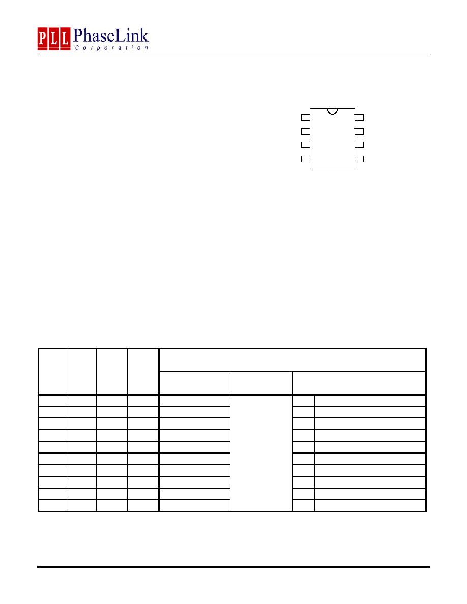
PIN CONFIGURATION
Note: ^: Internal pull-up resistor (120k
for SD, 30 k for
SC0-SC2).
*: The value of SD is latched upon power-up. The
internal pull-up resistor results in a default high value
when no pull-down resistor is connected to this pin
(recommended external pull-down resistor of 27 k
).
OUTPUT CLOCK SELECTION
SST Modulation
SD SC2
SC1
SC0
Magnitude Freq.
Type
0 1 1 0
3.75%
D
-3.75%
1 0 0 1
3.50%
D
-3.50%
1 0 1 0
3.75%
A
+0.125%,
-3.625%
1 1 0 0
3.25%
D
-3.25%
1 1 0 1
3.50%
A
+0.125%,
-3.375%
1 1 1 0
3.75%
A
+0.25%,
-3.5%
0 0 0 0
3.25%
C
+/-1.625
%
0 0 0 1
3.50%
C
+/-1.75%
0 0 1 0
3.75%
C
+/-1.875%
0 0 1 1
0.00%
Fin / 512
SST
OFF
Notes: A: Asymmetric Spread. D: Down Spread. C: Center Spread.
PL
L
7
01-3
1
1
2
3
4
5
6
7
8
XIN/FIN
XOUT/SD*^
SC0^
SC1^
VDD
FOUT
GND
SC2^
XIN/FIN = 10 ~ 30 MHz
PLL701-31
Low EMI Spread Spectrum Multiplier Clock
47745 Fremont Blvd., Fremont, California 94538 Tel (510) 492-0990 Fax (510) 492-0991
www.phaselink.com
Rev 11/28/05 Page 2
BLOCK DIAGRAM
PIN DESCRIPTIONS
Name Number
Type
Description
XIN/FIN 1 I
Crystal input to be connected to fundamental parallel mode crystal.(C
L
=18pF) or
clock input.
XOUT/SD 2 B
At power-up, this pin is an input pin to select modulation magnitude and type.
After input sampling, this pin is crystal output. Has internal pull up resistor.
SC0 3 I
Digital control input to select modulation magnitude and type.
Has internal pull-up.
SC1 4 I
Digital control input to select modulation magnitude and type.
Has internal pull-up.
SC2 7 I
Digital control input to select modulation magnitude and type.
Has internal pull-up.
VDD
8
P
3.0(+/-10%)V Power Supply.
FOUT
6
O
Modulated Clock Frequency Output.
GND 5 P
Ground.
XTAL
OSC
FOUT
XIN/FIN
XOUT
SC(0:2)
SD
PLL
SST
Control
Logic
PLL701-31
Low EMI Spread Spectrum Multiplier Clock
47745 Fremont Blvd., Fremont, California 94538 Tel (510) 492-0990 Fax (510) 492-0991
www.phaselink.com
Rev 11/28/05 Page 3
FUNCTIONAL DESCRIPTION
Selectable spread spectrum modulation types and magnitudes
The PLL701-31 provides selectable spread spectrum modulation type, as well as selectable modulation
magnitude. Selection is made by connecting specific pins to a logical "zero" or "one", according to the output
clock selection table on page 1.
In order to reduce the number of pins on the chip, the PLL701-31 uses pin 2 (XOUT/SD) as a bi-directional pin.
The pin serves as a modulation type and magnitude selector input (SD) upon power-up (see output clock
selection table on page 1), and as XOUT crystal connection as soon as the input has been latched.
Pins 3 (SC0), 4 (SC1), and 7 (SC2) are used as inputs to complete the spread spectrum modulation type and
magnitude selection as shown on the output clock selection table (page 1).
Connecting a selection pin to a logical "one"
All selection pins have an internal pull-up resistor (30k
for pins 3, 4, 7, and 120k for pin 2). This internal pull-
up resistor will pull the input value to a logical "one" by default, i.e. when no connection is made between the pin
and GND. No external pull-up resistor is therefore required for connecting a logical "one" upon power-up.
Connecting a selection pin to a logical "zero"
For an input only pin, i.e. pins 3 (SC0), 4 (SC1), and 7 (SC2), the pin simply needs to be grounded to pull the
input down to a logical "zero". Pin 2 (XOUT/SD) should be connected to GND thru a 27k
resistor to select a
logical "zero".
ELECTRICAL SPECIFICATIONS
1. Absolute Maximum Ratings
PARAMETERS SYMBOL
MIN.
MAX.
UNITS
Supply Voltage
V
DD
4.6 V
Input Voltage, dc
V
I
-0.5
V
DD
+0.5 V
Output Voltage, dc
V
O
-0.5
V
DD
+0.5 V
Storage Temperature
T
S
-65 150
∞C
Ambient Operating Temperature*
T
A
-40 85
∞C
Junction Temperature
T
J
125
∞C
Lead Temperature (soldering, 10s)
260
∞C
ESD Protection, Human Body Model
2
kV
Exposure of the device under conditions beyond the limits specified by Maximum Ratings for extended periods may cause permanent damage to the
device and affect product reliability. These conditions represent a stress rating only, and functional operations of the device at these or any other
conditions above the operational limits noted in this specification is not implied.
* Note: Operating Temperature is guaranteed by design for all parts (COMMERCIAL and INDUSTRIAL), but tested for COMMERCIAL grade only.
PLL701-31
Low EMI Spread Spectrum Multiplier Clock
47745 Fremont Blvd., Fremont, California 94538 Tel (510) 492-0990 Fax (510) 492-0991
www.phaselink.com
Rev 11/28/05 Page 4
2. DC/AC Specifications
PARAMETERS SYMBOL CONDITIONS MIN.
TYP.
MAX.
UNITS
Supply Voltage
V
DD
2.7 3.0 3.3 V
Input High Voltage
V
IH
0.7*
V
DD
V
Input Low Voltage
V
IL
0.3*
V
DD
V
Input High Current
I
IH
100
µA
Input Low Current
I
IL
100
µA
Output High Voltage
V
OH
I
OH
=5mA, V
DD
=3.3V
2.4
Output Low Voltage
V
OL
I
OL
=6mA, V
DD
=3.3V 0.4
F
XIN
When using a crystal
10
30
MHz
Input Frequency
F
IN
When using reference clock
10
30
MHz
Maximum interruption of F
IN
When using reference clock
100
µs
Load Capacitance
C
L
Between Pin XIN and
XOUT*
18 pF
Pull-up Resistor
R
up
PIN
2
120 k
Pull-up Resistor
R
up
PIN 3, 4, 7
30
k
Short Circuit Current
I
sc
50 mA
3.3V Dynamic Supply Current
I
CC
No
Load
18 mA
*Note: Pin XIN and XOUT each has a 36pF capacitance. When used with a XTAL, the two capacitors combined load the crystal with 18pF. If driving
XIN with a reference clock signal, the load capacitance will be 36pF (typical).
3. Timing Characteristics
PARAMETERS SYMBOL
CONDITIONS
MIN.
TYP.
MAX.
UNITS
Rise Time
T
r
Measured at 0.8V ~ 2.0V @ 3.3V
0.8
0.95
1.1
ns
Fall Time
T
f
Measured at 2.0V ~ 0.8V @ 3.3V
0.78
0.85
0.9
ns
Output Duty Cycle
D
T
45 50 55 %
Cycle to Cycle Jitter
T
cyc-cyc
FOUT=48MHz @ 3.3V
100
ps
Cycle to Cycle Jitter
T
cyc-cyc
FOUT=72MHz @ 3.3V
100
ps
PLL701-31
Low EMI Spread Spectrum Multiplier Clock
47745 Fremont Blvd., Fremont, California 94538 Tel (510) 492-0990 Fax (510) 492-0991
www.phaselink.com
Rev 11/28/05 Page 5
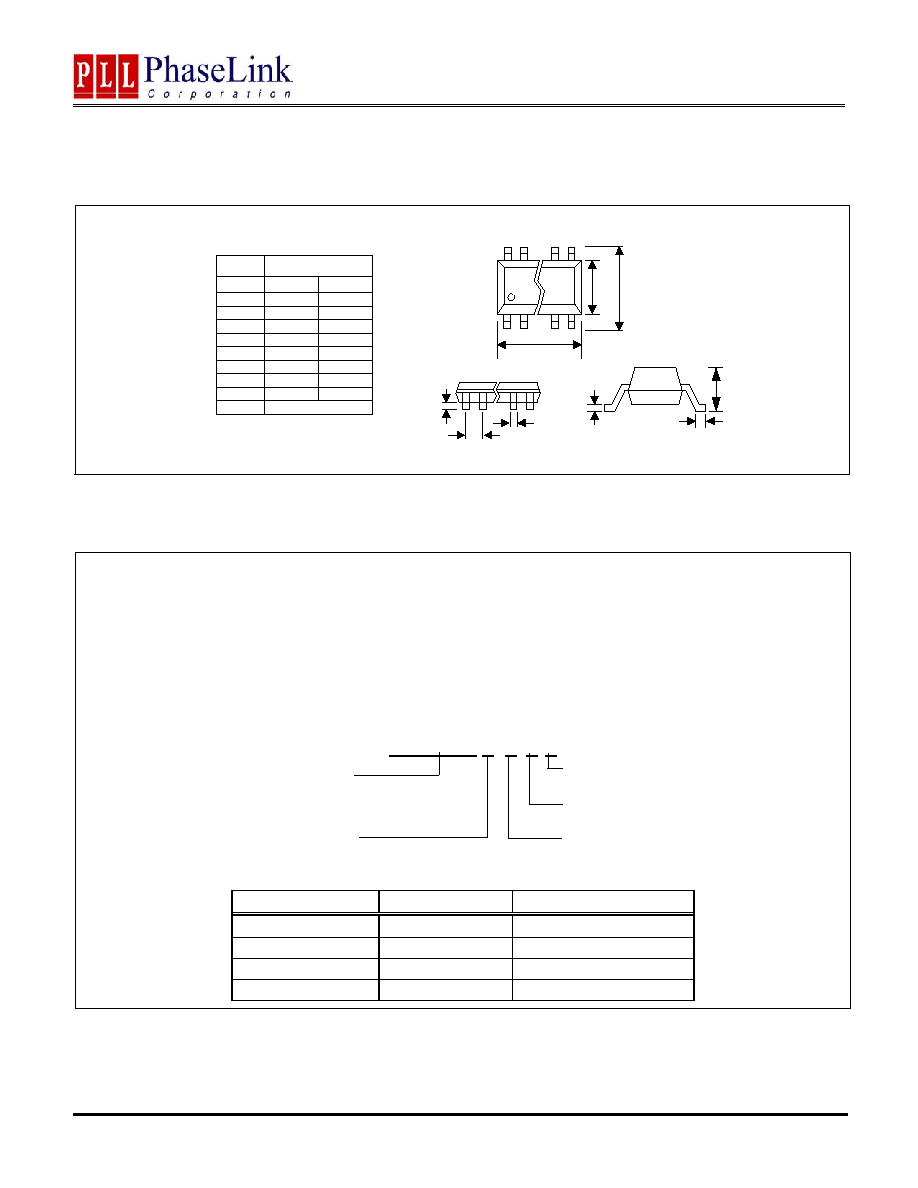
PACKAGE INFORMATION
ORDERING INFORMATION
PhaseLink Corporation, reserves the right to make changes in its products or specifications, or both at any time without notice. The information
furnished by Phaselink is believed to be accurate and reliable. However, PhaseLink makes no guarantee or warranty concerning the accuracy of said
information and shall not be responsible for any loss or damage of whatever nature resulting from the use of, or reliance upon this product.
LIFE SUPPORT POLICY: PhaseLink's products are not authorized for use as critical components in life support devices or systems without the
express written approval of the President of PhaseLink Corporation.
For part ordering, please contact our Sales Department:
47745 Fremont Blvd., Fremont, CA 94538, USA
Tel: (510) 492-0990 Fax: (510) 492-0991
PART NUMBER
The order number for this device is a combination of the following:
Device number, Package type and Operating temperature range
PLL701-31 S C
X
X
Order Number
Marking
Package Option
PLL701-31SC P701-31SC
SOIC-Tube
PLL701-31SC-R P701-31SC
SOIC-Tape
and
Reel
PLL701-31SCL P701-31SCL
SOIC-Tube
(GREEN)
PLL701-31SCL-R P701-31SCL
SOIC-Tape and Reel (GREEN)
C
L
A
8 PIN Narrow SOIC ( mm )
SOIC
Symbol
Min.
Max.
A
1.47
1.73
A1
0.10
0.25
B
0.33
0.51
C
0.19
0.25
D
4.80
4.95
E
3.80
4.00
H
5.80
6.20
L
0.38
1.27
e
1.27 BSC
E
H
D
A1
e
B
PART NUMBER
TEMPERATURE
C=COMMERCIAL
I=INDUSTRIAL
PACKAGE TYPE
S=SOIC
NONE= NORMAL PACKAGE
L= GREEN PACKAGE
NONE= TUBE
R= TAPE AND REEL