Preliminary
PLL702-03
Low EMI Peripheral Clock Generator for Notebook PCs
47745 Fremont Blvd., Fremont, California 94538 TEL (510) 492-0990 FAX (510) 492-0991 Rev 10/06/02 Page 1
FEATURES
∑
Single Low EMI IC to replace multiple crystals and
oscillators on Notebooks and Motherboards (27MHz,
8MHz, 12MHz, 24.576MHz, 25MHz).
∑
Single crystal input: 24.576MHz (accuracy requirement
+/- 20ppm)
∑
Less than 10ppm Frequency Synthesis error, meeting
AC97, IEEE1394, IEEE802 and USB2.0 frequency
precision specification.
∑
27MHz clock with 5 levels of Selectable Spread
Spectrum modulation form +/- 0.5% to +/- 1.5% center.
∑
25MHz clock with double drive strength (Ethernet PHY
and MAC).
∑
24.576MHz clocks for Audio Codec and IEEE1394.
∑
Selectable 12MHz (USB 2.0) or 8MHz (Keyboard
controller).
∑
Dual power source selection for 24.576MHz, 8MHz, and
12MHz.
∑
Available in 16-Pin SOIC or TSSOP.
Table 1. SPREAD SPECTRUM SELECTION
SST1
SST0
SST Modulation only on
27MHz. (pin 15)
1
1
+/- 1.5 %
1
0
+/- 1.25 %
1
M
+/- 1 %
0
1
+/- 0.75 %
0
0
+/- 0.5 %
0
M
SST OFF (Default)
Notes: M = Do not connect. 1 = Pulled up. 0 = Pulled down.
Table 2. POWER SELECTION TABLE
VDD_SEL
24.576MHz
(pin 7)
12MHz (pin 12)
8MHz (pin 13)
0
VDDB1
VDDB2
1
VDD25M
VDD25M
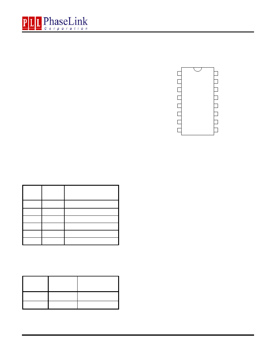
PIN ASSIGNMENT
POWER GROUPS
∑
VDDOSC ≠ VSSOSC: XIN, XOUT, analog core and
digital part.
∑
VDDB1 ≠ VSSB1: 24.576MHz.
∑
VDDB2 ≠ VSSB2: 27MHz, 8MHz, and 12MHz.
∑
VDD25M ≠ VSS25M: 25MHz, (also used for 12MHz,
8MHz when power VDDB2 is not present, and
24.576MHz when power VDDB1 is not present).
PLL 702-03
1
2
3
4
5
6
7
8
VDDOSC
9
10
11
12
13
14
15
16
XIN
XOUT
VSSOSC
VSSB1
24.576MHz/SST0*
T
24.576MHz/SST1*
v
VDDB1
VDDB2
27MHz
VSSB2
8MHz
12MHz/VDD_SEL*
v
VSS25M
25MHzx2
VDD25M
Note: 25MHzx2: double drive strength *: Bi-directional pin
v
: Internal pull-down resistor (120k
)
T
: Tri-level input

Preliminary
PLL702-03
Low EMI Peripheral Clock Generator for Notebook PCs
47745 Fremont Blvd., Fremont, California 94538 TEL (510) 492-0990 FAX (510) 492-0991 Rev 10/06/02 Page 2
BLOCK DIAGRAM
Note: In order to use VDD25M as power source for 8MHz (pin 13), 24.576MHz (pin 7), and 12MHz (pin 12), it is necessary to select this feature
through the VDD_SEL input (see Power Selection Table on p.1).
Note 2: Only 27MHz output is modulated for low EMI via Spread Spectrum.
SSC(0:1)
PLL2
25MHz
27_14.318MHz
VDDB2
VDD25M
XTAL
OSC
XIN
XOUT
PLL
SST
24.576MHz
(pin7)
VDDB1
12MHz
VDDB2
8MHz
VDDB2
VDD25M
24.576MHz
(pin6)
VDDB1
VDD25M
VDD25M

Preliminary
PLL702-03
Low EMI Peripheral Clock Generator for Notebook PCs
47745 Fremont Blvd., Fremont, California 94538 TEL (510) 492-0990 FAX (510) 492-0991 Rev 10/06/02 Page 3
PIN DESCRIPTIONS
Name
Pin#
Type
Description
VDDOSC
1
P
3.3V power supply for oscillator, analog core and digital circuitry.
XIN
2
I
Crystal input: for 24.576MHz fundamental crystal (CL = 20pF, parallel resonant mode, +/-
20ppm). On-chip load capacitors: no external load capacitors required.
XOUT
3
O
Crystal output.
VSSOSC
4
P
Ground connection.
VSSB1
5
P
Ground connection.
24.576MHz/SST0
6
B
Bi-directional and Tri-Level pin. Upon power-on, the value of SST0 is latched in and used
to select the SST control (see Spread Spectrum selection table 1). Tri level input: M = Do
not connect, 1 = Pull up, 0 = Pull down. After power-up this pin acts as 24.576MHz output
clock.
24.576MHz/SST1
7
B
Bi-directional pin. Upon power-on, the value of SST1 is latched in and used to select the
SST control (see Spread Spectrum selection table 1). Internal pull down defaults SST1 to
0, use external pull-up to set to 1. After power-up this pin acts as 24.576MHz output clock.
VDDB1
8
P
3.3V power supply for 24.576MHz clock.
VDD25M
9
P
3.3V power supply for 25MHz, 8MHz, 12MHz, 24.576MHz.
25MHzx2
10
O
25MHz Ethernet output clock (double drive strength).
VSS25M
11
P
Ground connection.
12MHz/VDD_SEL
12
B
Bi-directional pin. Upon power-on, the value of VDD_SEL is latched in and used to select
the power (see Power Selection table 2 ). Internal pull down defaults SST1 to 0, use
external pull-up to set to 1. After power-up this pin acts as 12MHz output clock.
8MHz
13
O
8MHz output clock (for Keyboard controller).
VSSB2
14
P
Ground connection.
27MHz
15
O
27MHz output. This output can be modulated for low EMI using SST (Spread Spectrum
Technology).
VDDB2
16
P
3.3V power supply for 27MHz, 20MHz, 12MHz, and 24.576MHz.
FUNCTIONAL DESCRIPTION
Tri-level and two-level inputs
In order to reduce pin usage, the PLL702-02 uses tri-level input pins. These pins allow 3 levels for input selection: namely, 0 =
Connect to GND, 1 = Connect to VDD, M = Do not connect. Thus, unlike the two-level selection pins, the tri-level input pins are
in the "M" (mid) state when not connected. In order to connect a tri-level pin to a logical "zero", the pin must be connected to
GND. Likewise, in order to connect to a logical "one", the pin must be connected to VDD.

Preliminary
PLL702-03
Low EMI Peripheral Clock Generator for Notebook PCs
47745 Fremont Blvd., Fremont, California 94538 TEL (510) 492-0990 FAX (510) 492-0991 Rev 10/06/02 Page 4
Connecting a bi-directional pin
The PLL702-03 also uses bi-directional pins. The same pin serves as input upon power-up, and as output as soon as the inputs
have been latched. The value of the input is latched-in upon power-up. Depending on the pin (see pin description), the input can
be tri-level or a standard two-level. Unlike unidirectional pins, bi-directional pins cannot be connected directly to GND or VDD in
order to set the input to "0" or "1", since the pin also needs to serve as output. In the case of two level input pins, an internal pull-
up resistor is present. This allows a default value to be set when no external pull down resistor is connected between the pin
and GND (by definition, a tri-level input has a the default value of "M" (mid) if it is not connected). In order to connect a bi-
directional pin to a non-default value, the input must be connected to GND or VDD through an external pull-down/pull-up
resistor.
Note: when the output load presents a low impedance in comparison to the internal pull-up resistor, the internal pull-up resistor
may not be sufficient to pull the input up to a logical "one", and an external pull-up resistor may be required.
For bi-directional inputs, the external loading resistor between the pin and GND has to be sufficiently small (compared to the
internal pull-up resistor) so that the pin voltage be pulled below 0.8V (logical "zero"). In order to avoid loading effects when the
pin serves as output, the value of the external pull-down resistor should however be kept as large as possible. In general, it is
recommended to use an external resistor of around one sixth to one quarter of the internal pull-up resistor (see Application
Diagram).
Note: when the output is used to drive a load presenting an small resistance between the output pin and VDD, this resistance is
in essence connected in parallel to the internal pull-up resistor. In such a case, the external pull-down resistor may have to be
dimensioned smaller to guarantee that the pin voltage will be low enough achieve the desired logical "zero". This is particularly
true when driving 74FXX TTL components.
APPLICATION DIAGRAM: BI-DIRECTIONAL PINS WITH INTERNAL PULL-UP
Latch
Power Up
Reset
Jumper options
R
UP
/
4
Clock Load
Latched
Input
Output
EN
VDD
R
up
Bi-directional pin
R
RB
NOTE: Rup=Internal pull-up resistor (see pin description). Power-up Reset : R starts from 1 to 0 while RB starts from 0 to 1.
Internal to chip
External Circuitry

Preliminary
PLL702-03
Low EMI Peripheral Clock Generator for Notebook PCs
47745 Fremont Blvd., Fremont, California 94538 TEL (510) 492-0990 FAX (510) 492-0991 Rev 10/06/02 Page 5
Electrical Specifications
1. Absolute Maximum Ratings
PARAMETERS
SYMBOL
MIN.
MAX.
UNITS
Supply Voltage Range
V
CC
-
0.5
7
V
Input Voltage Range
V
I
-
0.5
V
CC
+
0.5
V
Output Voltage Range
V
O
-
0.5
V
CC
+
0.5
V
Soldering Temperature
260
∞
C
Storage Temperature
T
S
-65
150
∞
C
Ambient Operating Temperature*
T
A
-40
85
∞
C
Exposure of the device under conditions beyond the limits specified by Maximum Ratings for extended periods may cause
permanent damage to the device and affect product reliability. These conditions represent a stress rating only, and functional
operations of the device at these or any other conditions above the operational limits noted in this specification is not implied.
* Note: Operating Temperature is guaranteed by design for all parts (COMMERCIAL and INDUSTRIAL), but tested for
INDUSTRIAL grade only.
2. AC Specification
PARAMETERS
CONDITIONS
MIN.
TYP.
MAX. UNITS
Input Frequency (to be set via XTAL_SEL)
+/- 20ppm accuracy
24.576
MHz
SST modulation sweep rate
28
kHz
Output Rise Time
0.8V to 2.0V with no load
1.5
ns
Output Fall Time
2.0V to 0.8V with no load
1.5
ns
Duty Cycle
At VDD/2
45
50
55
%
Duty Cycle 8MHz clock
At VDD/2
43
50
57
%
Max. Absolute Period Jitter
Long term, No SST
150
ps
Max. Jitter, cycle to cycle
Long term + Short term
120
ps

Preliminary
PLL702-03
Low EMI Peripheral Clock Generator for Notebook PCs
47745 Fremont Blvd., Fremont, California 94538 TEL (510) 492-0990 FAX (510) 492-0991 Rev 10/06/02 Page 6
3. DC Specification
PARAMETERS
SYMBOL
CONDITIONS
MIN.
TYP.
MAX.
UNITS
Operating Voltage
V
DD
Nominal voltage 3.3V
2.97
3.63
V
Input High Voltage
V
IH
V
DD
/2
V
Input Low Voltage
V
IL
V
DD
/2
V
DD
/2 - 1
V
Input High Voltage
V
IH
For all Tri-level input
V
DD
-0.5
V
Input Low Voltage
V
IL
For all Tri-level input
0.5
V
Input High Voltage
V
IH
For all normal input
2
V
Input Low Voltage
V
IL
For all normal input
0.8
V
I
OH
= -30mA (normal drive)
Output High Voltage
V
OH
I
OH
= -60mA (double drive)
2.4
V
I
OL
= 30mA (normal drive)
Output Low Voltage
V
OL
I
OH
= -60mA (double drive)
0.4
V
Output High Voltage At
CMOS Level
V
OH
I
OH
= -8mA
V
DD
-0.4
V
Normal drive strength
30
Nominal Output Current
I
OUT
Double drive strength
60
mA
Operating Supply Current
I
DD
No Load
35
mA
Short-circuit Current
I
S
±
100
mA

Preliminary
PLL702-03
Low EMI Peripheral Clock Generator for Notebook PCs
47745 Fremont Blvd., Fremont, California 94538 TEL (510) 492-0990 FAX (510) 492-0991 Rev 10/06/02 Page 7
PACKAGE INFORMATION
ORDERING INFORMATION
PhaseLink Corporation, reserves the right to make changes in its products or specifications, or both at any time without notice. The information
furnished by Phaselink is believed to be accurate and reliable. However, PhaseLink makes no guarantee or warranty concerning the accuracy of said
information and shall not be responsible for any loss or damage of whatever nature resulting from the use of, or reliance upon this product.
LIFE SUPPORT POLICY: PhaseLink's products are not authorized for use as critical components in life support devices or systems without the
express written approval of the President of PhaseLink Corporation.
For part ordering, please contact our Sales Department:
47745 Fremont Blvd., Fremont, CA 94538, USA
Tel: (510) 492-0990 Fax: (510) 492-0991
PART NUMBER
The order number for this device is a combination of the following:
Device number, Package type and Operating temperature range
PLL702-03 X C
PART NUMBER
TEMPERATURATURE
C=COMMERCIAL
M=MILITARY
I=INDUSTRAL
PACKAGE TYPE
O = TSSOP, S = SOIC
C
L
A
16 PIN Narrow SOIC, TSSOP ( mm )
SOIC
TSSOP
Symbol
Min.
Max.
Min.
Max.
A
1.35
1.75
-
1.20
A1
0.10
0.25
0.05
0.15
B
0.33
0.51
0.19
0.30
C
0.19
0.25
0.09
0.20
D
9.80
10.00
4.90
5.10
E
3.80
4.00
4.30
4.50
H
5.80
6.20
6.40 BSC
L
0.40
1.27
0.45
0.75
e
1.27 BSC
0.65 BSC
E
H
D
A1
e
B