FEATURES
∑
Single Power Supply Operation
- 5.0 V ± 10% Read/Program/Erase
∑ High Performance Read
- 70/90 ns access time
∑ Memory Blocks Architecture
- One 16 Kbytes top or bottom Boot Block with
software lockout
- Two 8 Kbytes Parameter Blocks
- One 96 Kbytes Main Block
- Three 128 Kbytes Main Blocks
∑ Automatic Block Erase and Byte Program
- Typical 12
µ
s/byte programming
- Typical 50 ms block or chip erase
∑ Hardware Data Protection
∑ Data# Polling and Toggle Bit Features
∑ Low Power Consumption
- Typical 15 mA active read current
- Typical 40 mA program/erase current
- Typical 0.1
µ
A CMOS standby current
∑ High Product Endurance
- Guarantee 10,000 program/erase cycles
- Typical 50,000 program/erase cycles
- Minimum 10 years data retention
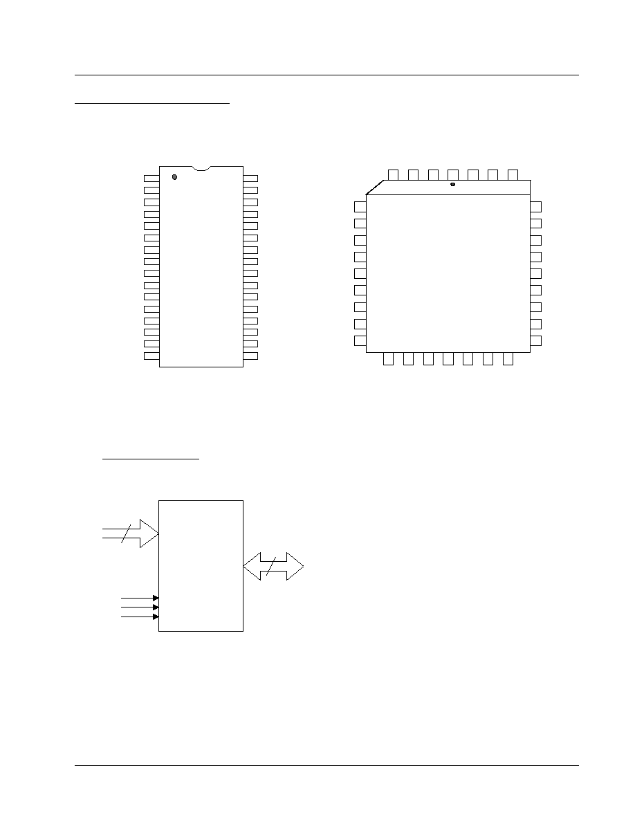
∑ Industrial Standard Pin-out and Packaging
- 32-pin Plastic DIP
- 32-pin PLCC
∑ Manufactured on 0.30 µm process
GENERAL DESCRIPTION
The Pm29F004 is a 4 Megabit, 5 Volt-only Flash Memory organized as 524,288 bytes of 8 bits each. This
device is designed to use a 5.0 Volt power supply to perform in-system programming, 12.0 Volt V
PP
power supply
for program and erase operation is not required. The device can be programmed in standard EPROM program-
mers as well.
The 4 Megabit memory array is divided into seven blocks of one 16 Kbytes, two 8 Kbytes, one 96 Kbytes,
and three 128 Kbytes for BIOS and parameters storage. The seven blocks allow users to flexibly make chip erase
or block erase operation. The block erase feature allows a particular block to be erased and reprogrammed
without affecting the data in other blocks. After the device performed chip erase or block erase operation, it can
be reprogrammed on a byte-by-byte basis.
The device has a standard microprocessor interface as well as JEDEC single-power-supply Flash compatible
pin-out and command set. The program operation of Pm29F004 is executed by issuing the program command
code into command register. The internal control logic automatically handles the programming voltage ramp-up
and timing. The erase operation of Pm29F004 is executed by issuing the chip erase or block erase command
code into command register. The internal control logic automatically handles the erase voltage ramp-up and
timing. The preprogramming on the array which has not been programmed is not required before the erase
operation. The device also features Data# Polling and Toggle Bit function, the end of program or erase operation
can be detected by Data# Polling of I/O7 or Toggle Bit of I/O6.
The device has an optional 16 Kbytes top or bottom boot block with a software lockout feature for data
security. The boot block can be used to store user secure code. When the lockout feature is enabled, the boot
block is permanently protected from being reprogrammed.
The Pm29F004 is manufactured on PMC's advanced 0.30 µm, P-FLASHTM, nonvolatile memory process.
The device is packaged in a 32-pin DIP and PLCC with access time of 70 and 90 ns.
PMC
4 Megabit (512K X 8) 5.0 Volt-only CMOS Flash Memory
Programmable Microelectronics Corp.
Issue Date: November, 2000 Rev:1. 0
PRELIMINARY
Pm29F004
1

Programmable Microelectronics Corp.
Issue Date: November, 2000 Rev: 1.0
PMC
Pm29F004 Preliminary
PRODUCT ORDERING INFORMATION
3
Pm29F004 T -70 P C
Temperature Range
C = Commercial (0∞C to +70∞C)
Package Type
P = 32-pin Plastic DIP (32P)
J = 32-pin Plastic J-Leaded Chip Carrier (32J)
Speed Option
Boot Block Location
T = Top Boot Block
B = Bottom Boot Block
PMC Device Number
r
e
b
m
u
N
t
r
a
P
t
C
C
A
)
s
n
(
t
o
o
B
n
o
i
t
a
c
o
L
e
g
a
k
c
a
P
e
r
u
t
a
r
e
p
m
e
T
e
g
n
a
R
C
J
0
7
-
T
4
0
0
F
9
2
m
P
0
7
p
o
T
J
2
3
l
a
i
c
r
e
m
m
o
C
)
C
∞
0
7
+
o
t
C
∞
0
(
C
P
0
7
-
T
4
0
0
F
9
2
m
P
P
2
3
C
J
0
7
-
B
4
0
0
F
9
2
m
P
m
o
t
t
o
B
J
2
3
C
P
0
7
-
B
4
0
0
F
9
2
m
P
P
2
3
C
J
0
9
-
T
4
0
0
F
9
2
m
P
0
9
p
o
T
J
2
3
l
a
i
c
r
e
m
m
o
C
)
C
∞
0
7
+
o
t
C
∞
0
(
C
P
0
9
-
T
4
0
0
F
9
2
m
P
P
2
3
C
J
0
9
-
B
4
0
0
F
9
2
m
P
m
o
t
t
o
B
J
2
3
C
P
0
9
-
B
4
0
0
F
9
2
m
P
P
2
3

Programmable Microelectronics Corp.
Issue Date: November, 2000 Rev: 1.0
PMC
Pm29F004 Preliminary
BLOCK DIAGRAM
DEVICE OPERATION
READ OPERATION
The access of Pm29F004 is similar as that of
EPROM. To obtain data at the outputs, three control
functions must be satisfied:
∑ CE# is the chip enable and should be pulled low
( V
IL
).
∑ OE# is the output enable and should be pulled
low ( V
IL
).
∑ WE# is the write enable and should remains high
( V
IH
)
.
BOOT BLOCK LOCKOUT
The device has a software lockout feature to pre-
vent the data in the boot block from being erased or
reprogrammed. The boot block can be located at the
top or bottom of the address location. The block size is
16 Kbytes. Once the lockout feature is enable, the boot
block can not be erased or reprogrammed. Data in the
main memory block can still be updated through the
regular programming method. The boot block lockout
feature can be turned on by issuing a six-bus-cycle com-
mand sequence. Please refer to Table 4 and Chart 4.
BOOT BLOCK LOCKOUT DETECTION
The state of the Boot Block lockout can be de-
tected by software product identification entry. After
entry, selects Boot Block address with A0 = "0" and A1
= "1" and then read I/O0. A data of "0" means the lock-
out feature is disabled and the Boot Block can be erased
or programmed. A data of "1" means the lockout fea-
ture is enabled and the Boot Block is protected. Prod-
uct identification exit must be executed before the de-
vice returns to read mode.
PRODUCT IDENTIFICATION
The product identification mode can be used to identify
the device and the manufacturer by hardware or soft-
ware operation. The hardware operation mode is acti-
vated by applying a 12.0 Volt on A9 pin, typically used
by an external programmer to select the right program-
ming algorithm for the device. For detail, please see
Bus Operation Modes in Table 3. The software opera-
tion mode is activated by three-bus-cycle command.
Please see Software Command Definition in Table 4.
5
W E #
C E #
O E #
C O M M A N D
R E G I S T E R
C E , O E L O G I C
A0-A18
E R A S E / P R O G R A M
V O L T A G E
G E N E R A T O R
H I G H V O L T A G E
S W I T C H
I/O0-I/O7
I / O B U F F E R S
D A T A
L A T C H
S E N S E
A M P
Y - G A T I N G
M E M O R Y
A R R A Y
ADDRESS
LATCH
Y - D E C O D E R
X - D E C O D E R