FEATURES
Single Power Supply Operation
- Low voltage range: 4.5 V - 5.5 V
∑ Memory Organization
- Pm39F010: 128K x 8 (1 Mbit)
- Pm39F020: 256K x 8 (2 Mbit)
- Pm39F040: 512K x 8 (4 Mbit)
∑ High Performance Read
- 55/70 ns access time
∑ Cost Effective Sector/Block Architecture
- Uniform 4 Kbyte sectors
- Uniform 64 Kbyte blocks (sector-group)
∑ Data# Polling and Toggle Bit Features
∑ Hardware Data Protection
∑ Automatic Erase and Byte Program
- Typical 16 µs/byte programming time
- Typical 55 ms sector/block/chip erase time
∑ Low Power Consumption
- Typical 8 mA active read current
- Typical 9 mA program/erase current
- Typical 0.5 µA CMOS standby current
∑ High Product Endurance
- Guarantee 100,000 program/erase cycles per
single sector (preliminary)
- Minimum 20 years data retention
∑ Industrial Standard Pin-out and Packaging
- 32-pin Plastic DIP
- 32-pin PLCC
- 32-pin VSOP (TSOP 8mm x 14mm)
- Optional lead-free (Pb-free) packages
GENERAL DESCRIPTION
The Pm39F010/020/040 are 1 Mbit/2 Mbit/4 Mbit 5.0 Volt-only Flash Memories. These devices are designed to use
a single low voltage, range from 4.5 Volt to 5.5 Volt, power supply to perform read, erase and program operations.
The 12.0 Volt V
PP
power supply for program and erase operations are not required. The devices can be programmed
in standard EPROM programmers as well.
The memory arrays of Pm39F010/020/040 are divided into uniform 4 Kbyte sectors or uniform 64 Kbyte blocks
(sector group - consists of sixteen adjacent sectors). The sector or block erase feature allows users to flexibly
erase an memory area as small as 4 Kbyte or as large as 64 Kbyte by one single erase operation without affecting
the data in others. The chip erase feature allows the whole memory array to be erased in one single erase opera-
tion. The devices can be programmed on a byte-by-byte basis after performing the erase operation.
The devices have a standard microprocessor interface as well as a JEDEC standard pin-out/command set. The
program operation is executed by issuing the program command code into command register. The internal control
logic automatically handles the programming voltage ramp-up and timing. The erase operation is executed by
issuing the chip erase, block, or sector erase command code into command register. The internal control logic
automatically handles the erase voltage ramp-up and timing. The preprogramming on the array which has not been
programmed is not required before an erase operation. The devices offer Data# Polling and Toggle Bit functions, the
progress or completion of program and erase operations can be detected by reading the Data# Polling on I/O7 or
the Toggle Bit on I/O6.
The Pm39F010/020/040 are manufactured on PMC's advanced nonvolatile CMOS technology, P-FLASHTM. The
devices are offered in 32-pin PDIP, PLCC and VSOP packages with access time of 55 and 70 ns.
PMC
1 Mbit / 2 Mbit / 4 Mbit 5 Volt-only CMOS Flash Memory
Programmable Microelectronics Corp.
Issue Date: March 2004, Rev:1.3
Pm39F010 / Pm39F020 / Pm39F040
1

Programmable Microelectronics Corp.
Issue Date: March, 2004, Rev: 1.3
PMC
Pm39F010 / Pm39F020 / Pm39F040
2
20
19
18
17
16
15
14
5
6
7
8
9
10
11
12
13
1
2
3
4
32
31
30
29
28
27
26
25
24
23
22
21
A14
A13
A 8
A 9
A11
O E #
A10
C E #
I/O7
A14
A13
A 8
A 9
A11
O E #
A10
C E #
I/O7
A14
A13
A 8
A 9
A11
O E #
A10
C E #
I/O7
I/O1
GND
I/O2
I/O3
I/O4
I/O5
I/O6
I/O1
GND
I/O2
I/O3
I/O4
I/O5
I/O6
I/O1
GND
I/O2
I/O3
I/O4
I/O5
I/O6
I/O0
A 0
A 1
A 2
A 3
A 4
A 5
A 6
A 7
I/O0
A 0
A 1
A 2
A 3
A 4
A 5
A 6
A 7
I/O0
A 0
A 1
A 2
A 3
A 4
A 5
A 6
A 7
A12
A15
V
CC
WE#
NC
NC
A12
A15
V
CC
WE#
A12
A15
V
CC
WE#
A16
A16
A16
A18
A17
A17
NC
39F010
39F020
39F040
39F040
39F020
39F010
3 9 F 0 1 0
3 9 F 0 2 0
3 9 F 0 4 0
3 9 F 0 4 0
3 9 F 0 2 0
3 9 F 0 1 0
32-Pin PLCC
CONNECTION DIAGRAMS
1
2
3
4
5
6
7
8
9
10
11
12
13
14
15
16
3 2
3 1
3 0
2 9
2 8
2 7
2 6
2 5
2 4
2 3
2 2
2 1
2 0
1 9
1 8
1 7
32-Pin VSOP
39F040
A 1 1
A 9
A 8
A 1 3
A 1 4
W E #
V
C C
A 1 5
A 1 2
A 7
A 6
A 5
A 4
A 1 6
A 1 8
A 1 7
39F020
A 1 1
A 9
A 8
A 1 3
A 1 4
W E #
V
C C
N C
A 1 5
A 1 2
A 7
A 6
A 5
A 4
A 1 6
A 1 7
39F010
A 1 1
A 9
A 8
A 1 3
A 1 4
W E #
V
C C
N C
A 1 5
A 1 2
A 7
A 6
A 5
A 4
A 1 6
N C
I / O 4
O E #
A 1 0
C E #
I / O 7
I / O 6
I / O 5
I / O 3
G N D
I / O 2
I / O 1
I / O 0
A 0
A 1
A 2
A 3
39F040
I / O 4
O E #
A 1 0
C E #
I / O 7
I / O 6
I / O 5
I / O 3
G N D
I / O 2
I / O 1
I / O 0
A 0
A 1
A 2
A 3
39F020
I / O 4
O E #
A 1 0
C E #
I / O 7
I / O 6
I / O 5
I / O 3
G N D
I / O 2
I / O 1
I / O 0
A 0
A 1
A 2
A 3
39F010
Programmable Microelectronics Corp.
Issue Date: March, 2004, Rev: 1.3
PMC
Pm39F010 / Pm39F020 / Pm39F040
3
CONNECTION DIAGRAMS (CONTINUED)
32-Pin PDIP
3 2
3 1
3 0
2 9
2 8
2 7
2 6
2 5
2 4
2 3
2 2
2 1
2 0
1 9
1 8
1 7
1
2
3
4
5
6
7
8
9
1 0
1 1
1 2
1 3
1 4
1 5
1 6
N C
A 1 6
A 1 5
A 1 2
A 7
A 6
A 5
A 4
A 3
A 2
I/O0
I/O1
A 1
A 0
I/O2
G N D
V
C C
W E #
N C
A 1 4
A 1 3
A 8
A 9
O E #
A 1 0
A 1 1
C E #
I/O7
I/O6
I/O5
I/O4
I/O3
3 9 F 0 1 0
V
C C
W E #
A 1 4
A 1 3
A 8
A 9
O E #
A 1 0
A 1 1
C E #
I/O7
I/O6
I/O5
I/O4
I/O3
3 9 F 0 2 0
V
C C
W E #
A 1 4
A 1 3
A 8
A 9
O E #
A 1 0
A 1 1
C E #
I/O7
I/O6
I/O5
I/O4
I/O3
3 9 F 0 4 0
A 1 7
A 1 7
3 9 F 0 1 0
N C
A 1 6
A 1 5
A 1 2
A 7
A 6
A 5
A 4
A 3
A 2
I/O0
I/O1
A 1
A 0
I/O2
G N D
3 9 F 0 2 0
A 1 8
A 1 6
A 1 5
A 1 2
A 7
A 6
A 5
A 4
A 3
A 2
I/O0
I/O1
A 1
A 0
I/O2
G N D
3 9 F 0 4 0
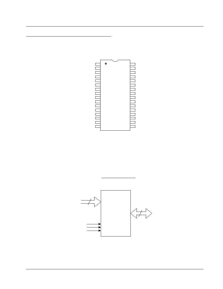
8
A 0 - A
M S
I/O0-I/O7
C E #
O E #
W E #
LOGIC SYMBOL
Note: A
MS
is the most significant address where A
MS
= A16 for Pm39F010, A17 for Pm39F020,
and A18 for Pm39F040.

Programmable Microelectronics Corp.
Issue Date: March, 2004, Rev: 1.3
PMC
Pm39F010 / Pm39F020 / Pm39F040
4
PRODUCT ORDERING INFORMATION
Pm39F0x0 -70 J C E
Temperature Range
C = Commercial (0∞C to +85∞C)
Package Type
J = 32-pin Plastic J-Leaded Chip Carrier (32J)
V = 32-pin Thin Small Outline Package (32V)
P = 32-pin Plastic DIP (32P)
Speed Option
- 70 = 70ns
- 55 = 55ns
PMC Device Number
Pm39F010 (1 Mbit)
Pm39F020 (2 Mbit)
Pm39F040 (4 Mbit)
Environmental Attribute
E = Lead-free (Pb-free) Package
Blank = Standard Package