PMC-930909 (R7)
PROPRIETARY AND CONFIDENTIAL TO PMC-SIERRA, INC., AND FOR ITS CUSTOMERS' INTERNAL USE
1998 PMC-Sierra, Inc. October,
PM5347
PMC-Sierra,Inc.
155 Mb/s SATURN User Network Interface for WANs
S/UNI-155-PLUS
FEATURES
∑ Monolithic SATURNTM-compatible
Asynchronous Transfer Mode (ATM)
network interface.
∑ Implements the ATM transmission
convergence (TC) sublayer for ATM
according to ATM Forum specifications
and ITU-T recommendations using the
SONET/SDH 155.52 Mb/s format. Also
implements ATM Forum specified
"Mid-range PHY" rates of 51.52, 25.92
and 12.96 Mb/s.
∑ Includes on-chip clock recovery and
clock synthesis at all rates. Clocking
can be bypassed for use with external
clock sources. Operates in master or
slave (loop timed) timing modes.
∑ Provides TTL-compatible inputs and
outputs. Provides differential pseudo-
ECL-compatible serial line side inputs.
∑ Supports Fiber Optic, Unshielded
Twisted Pair and Shielded interfaces.
∑ Processes all SONET/SDH UNI
overhead.
∑ Provides access to section and line
datalinks and all additional transport
and path overhead to allow additional
external processing for full SONET/
SDH Network-Node Interface (NNI)
compliance.
∑ Provides synchronous 8-bit or 16-bit
SCI-PHYTM system side interface with
4-cell deep FIFO buffers in transmit
and receive paths with parity support.
∑ Inserts and extracts ATM payloads
using cell delineation.
∑ Provides a generic 8-bit
microprocessor bus interface for
configuration, control, and status
monitoring.
∑ Software-compatible with the PM5345
S/UNI-155TM, PM5346 S/UNI-155-
LITETM and the PM5355 S/UNI-622TM.
∑ Provides a standard 5-signal P1149.1
JTAG test port for boundary scan
board test purposes.
∑ Low power, +5 V CMOS technology.
∑ Packaged in a 208 pin (28mm x
28mm) PQFP with 0.5mm pin pitch.
∑ Industrial temperature range operation
(-40
∞
C to +85
∞
C).
∑ Counts received cells written into the
receive FIFO, received HCS errored
cells that are discarded, and received
HCS errored cells that are corrected
and passed through the receive FIFO.
TRANSMIT SECTION
∑ Counts transmit cells read from the
transmit FIFO.
∑ Inserts a register programmable path
signal label (C2).
∑ Inserts path B3, path FEBE
indications, line B2, line FEBE
indications, and section B1 to allow
performance monitoring at the far end.
∑ Optionally inserts the 16- or 64-byte
section trace (J0) sequence and the 16
or 64 byte path trace (J1) sequence
from internal register banks.
∑ Optionally inserts an externally
generated section user channel (F1),
order wire channels (E1, E2) and the
DCC channels (D1-D3 and D4-D12)
via serial interfaces.
∑ Optionally inserts path AIS, path RDI,
line AIS, and line RDI.
∑ Optionally inserts register
programmable APS (K1, K2) and
synchronization status (Z1) bytes.
RECEIVE SECTION
∑ Filters and captures the automatic
protection switch channel (K1, K2)
bytes in readable registers and detects
APS byte failure.
∑ Extracts the 16- or 64-byte section
trace (J0) sequence and the 16- or 64-
byte path trace (J1) sequence into
internal register banks.
∑ Extracts the DCC channels (D1-D3
and D4-D12) for optional external
processing.
∑ Detects Loss Of Signal (LOS), Out Of
Frame (OOF), Loss Of Frame (LOF),
line Alarm Indication Signal (AIS), line
Remote Defect Indication (RDI-L),
Loss Of Pointer (LOP), path AIS, path
RDI (RDI-P) and Loss Of Cell
Delineation (LCD).
∑ Counts received section B1 errors, line
B2 errors, line FEBEs, path B3 errors
and path FEBEs for performance
monitoring purposes.
APPLICATIONS
∑ ATM Switching Systems
∑ ATM Access Systems
∑ LAN Switches, Hubs and Routers
∑ ATM Test Equipment
∑ SONET or SDH ATM Interfaces
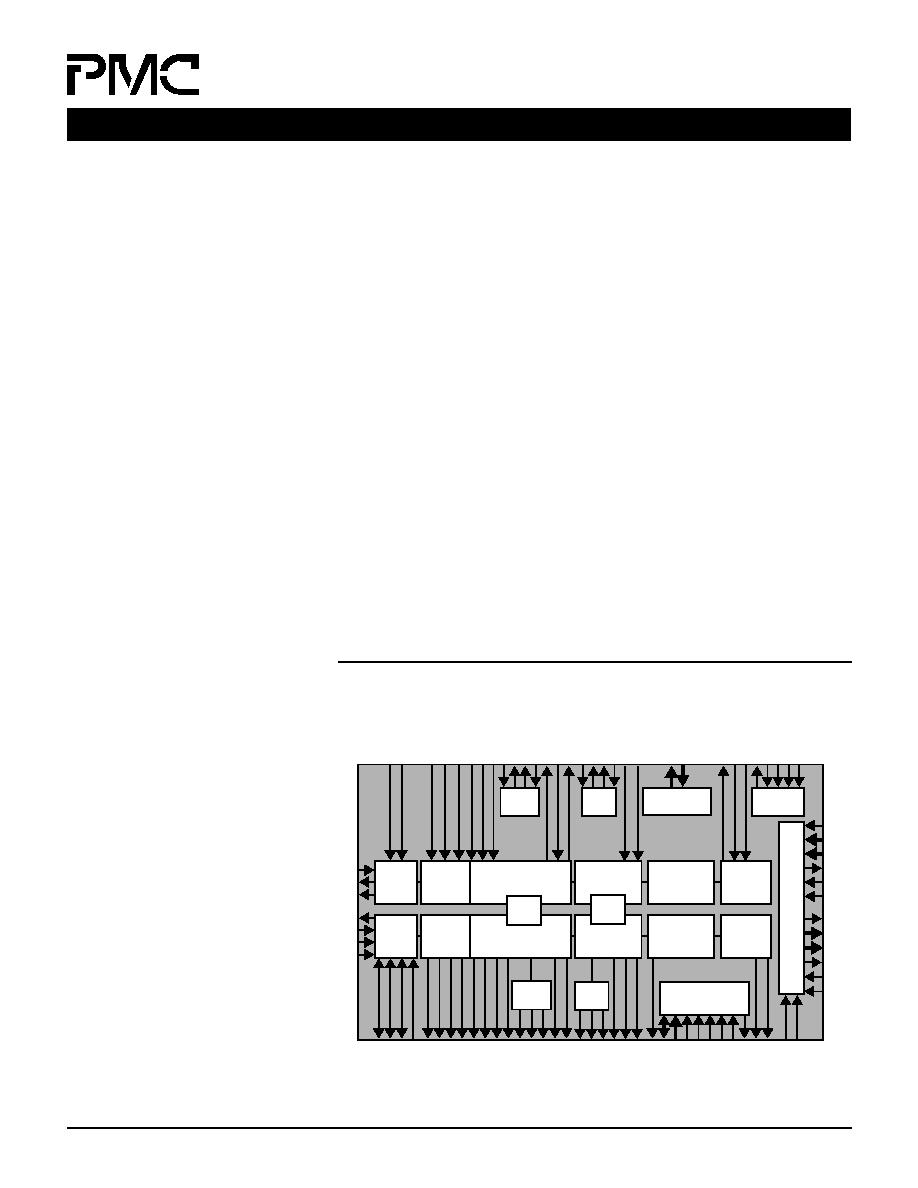
BLOCK DIAGRAM
Microprocessor
Interface
ALOS+/-
RRCLK+/-
Line Side
System Side
LF
+
/
-
FL
O
RA
T
P
R
BYP
LO
S
LOF
RS
DCLK
,
RO
WCLK
RS
D,
RS
O
W
,RS
U
C
LA
I
S
LRDI
RLDCLK
RLD,
RLO
W
RT
O
H
RT
O
H
F
P
RT
O
HCLK
RP
O
H
RP
O
H
F
P
RP
O
C
LK
LC
D
D[
7:
0]
A
[
7:
0]
AL
E
CS
B
WRB
RDB
RS
T
B
IN
T
B
RCP
RG
F
C
Path
O/H
Extract
Transport
O/H
Extract
TCA
TWRENB
TFCLK
TDAT[15:0]
TXPRTY[1:0]
TSOC
RCA
RRDENB
RFCLK
RDAT[15:0]
RSOC
Drop
Side
I/F
Receive
ATM 4-Cell
FIFO
Transmit
ATM 4-Cell
FIFO
Clock
Recovery
SIPO
RO
HF
P
GR
O
C
LK
Receive
Section O/H
Processor
LO
P
P
RDI
PYE
L
Transmit
Section O/H
Processor
Path
O/H
Extract
Transport
O/H
Extract
JTAG Test
Access Port
Parallel
Input/Output Port
T
S
DCL
K
,
T
O
WCLK
TS
D
,
T
S
O
W
,
T
S
U
C
T
L
DCLK
T
L
RDI
TOH
F
P
GT
O
C
L
K
PO
P[3
:
0
]
P
I
P
[
3:
0]
TP
OH
TP
OH
F
P
T
P
O
HCLK
TP
OH
E
N
TD
O
TD
I
TC
K
TM
S
TR
S
T
B
Clock
Recovery
SIPO
RXDO+/-
RXD+/-
TA
T
P
TB
Y
P
TL
A
I
S
TT
OH
TT
OH
F
P
T
T
O
HCLK
TT
OH
E
N
TP
A
I
S
T
P
RDI
TC
P
TG
F
C
XO
F
F
TL
D
,
TL
O
W
GT
O
C
L
K
BU
S8
T
SEN
TXC+/-
TRCLK+/-
TXD+/-
RXPRTY[1:0]
Receive
Path Overhead
Processor
Transmit
Path Overhead
Processor
Receive
ATM
Cell Processor
Transmit
ATM
Cell Processor
Receive
Line O/H
Processor
Transmit
Line O/H
Processor
Path
Trace
Buffer
Section
Trace
Buffer

Head Office:
PMC-Sierra, Inc.
#105 - 8555 Baxter Place
Burnaby, B.C. V5A 4V7
Canada
Tel: 604.415.6000
Fax: 604.415.6200
PM5347 S/UNI-155-PLUS
155 Mb/s SATURN User Network Interface for WANs
To order documentation,
send email to:
document@pmc-sierra.com
or contact the head office,
Attn: Document Coordinator
All product documentation is
available on our web site at:
http://www.pmc-sierra.com
For corporate information,
send email to:
info@pmc-sierra.com
PMC-930909 (R7)
1998 PMC-Sierra, Inc.
October, 1998
SATURN, SCI-PHY, S/UNI-155,
S/UNI-155-LITE, S/UNI-155-PLUS, and
S/UNI-622 are trademarks of PMC-Sierra, Inc.
PROPRIETARY AND CONFIDENTIAL TO PMC-SIERRA, INC., AND FOR ITS CUSTOMERS' INTERNAL USE
TYPICAL APPLICATION
155 Mb/s ATM SWITCH PORT INTERFACE
STS-3C/STM-1 OVERHEAD BYTE USAGE
Transmit
Alarm Insert
Signals
Receive
Alarm Detect
Signals
Receive
Overhead
Extract
PM5347
681,3/86
TM
155 Mb/s SATURN
TM
User Network Inter-
face for WANs
TCA
Transmit
ATM
Process
TXPRTY[1:0]
TDAT[15:0]
TSOC
TWRENB
TFCLK
RXPRTY[1:0]
RDAT[15:0]
RSOC
RFCLK
RRDENB
RCA
Switching
Network
Receive
ATM
Process
Microprocessor Bus for Configu-
ration, Status, and Control
Transmit
Overhead
Insert
O/E
Reference
Clock
TRCLK+/-
TXD+/-
RRCLK+/-
RXD+/-
ALOS+/-
E/O