 | –≠–ª–µ–∫—Ç—Ä–æ–Ω–Ω—ã–π –∫–æ–º–ø–æ–Ω–µ–Ω—Ç: BDW53C | –°–∫–∞—á–∞—Ç—å:  PDF PDF  ZIP ZIP |
BDW53, BDW53A, BDW53B, BDW53C, BDW53D
NPN SILICON POWER DARLINGTONS
P R O D U C T I N F O R M A T I O N
1
AUGUST 1978 - REVISED MARCH 1997
Copyright © 1997, Power Innovations Limited, UK
Information is current as of publication date. Products conform to specifications in accordance
with the terms of Power Innovations standard warranty. Production processing does not
necessarily include testing of all parameters.
q
Designed for Complementary Use with
BDW54, BDW54A, BDW54B, BDW54C and
BDW54D
q
40 W at 25∞C Case Temperature
q
4 A Continuous Collector Current
q
Minimum h
FE
of 750 at 3 V, 1.5 A
B
C
E
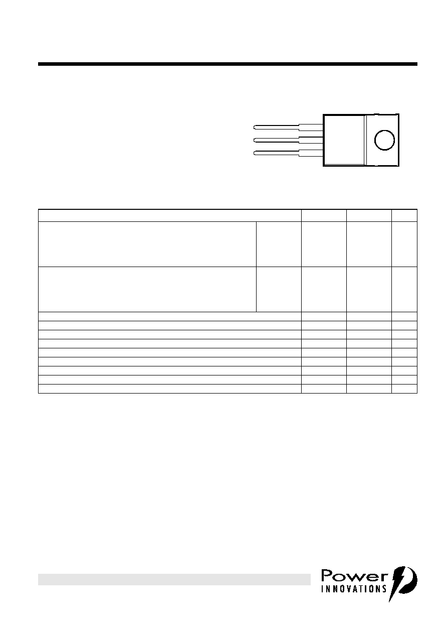
TO-220 PACKAGE
(TOP VIEW)
Pin 2 is in electrical contact with the mounting base.
MDTRACA
1
2
3
absolute maximum ratings
at 25∞C case temperature (unless otherwise noted)
NOTES: 1. These values apply when the base-emitter diode is open circuited.
2. Derate linearly to 150∞C case temperature at the rate of 0.32 W/∞C.
3. Derate linearly to 150∞C free air temperature at the rate of 16 mW/∞C.
4. This rating is based on the capability of the transistor to operate safely in a circuit of: L = 20 mH, I
B(on)
= 5 mA, R
BE
= 100
,
V
BE(off)
= 0, R
S
= 0.1
, V
CC
= 20 V.
RATING
SYMBOL
VALUE
UNIT
Collector-base voltage (I
E
= 0)
BDW53
BDW53A
BDW53B
BDW53C
BDW53D
V
CBO
45
60
80
100
120
V
Collector-emitter voltage (I
B
= 0) (see Note 1)
BDW53
BDW53A
BDW53B
BDW53C
BDW53D
V
CEO
45
60
80
100
120
V
Emitter-base voltage
V
EBO
5
V
Continuous collector current
I
C
4
A
Continuous base current
I
B
50
mA
Continuous device dissipation at (or below) 25∞C case temperature (see Note 2)
P
tot
40
W
Continuous device dissipation at (or below) 25∞C free air temperature (see Note 3)
P
tot
2
W
Unclamped inductive load energy (see Note 4)
ΩLI
C
2
25
mJ
Operating junction temperature range
T
j
-65 to +150
∞C
Operating temperature range
T
stg
-65 to +150
∞C
Operating free-air temperature range
T
A
-65 to +150
∞C
BDW53, BDW53A, BDW53B, BDW53C, BDW53D
NPN SILICON POWER DARLINGTONS
2
AUGUST 1978 - REVISED MARCH 1997
P R O D U C T I N F O R M A T I O N
NOTES: 5. These parameters must be measured using pulse techniques, t
p
= 300 µs, duty cycle
2%.
6. These parameters must be measured using voltage-sensing contacts, separate from the current carrying contacts.
Voltage and current values shown are nominal; exact values vary slightly with transistor parameters.
electrical characteristics at 25∞C case temperature (unless otherwise noted)
PARAMETER
TEST CONDITIONS
MIN
TYP
MAX
UNIT
V
(BR)CEO
Collector-emitter
breakdown voltage
I
C
= 30 mA
I
B
= 0
(see Note 5)
BDW53
BDW53A
BDW53B
BDW53C
BDW53D
45
60
80
100
120
V
I
CEO
Collector-emitter
cut-off current
V
CE
= 30 V
V
CE
= 30 V
V
CE
= 40 V
V
CE
= 50 V
V
CE
= 60 V
I
B
= 0
I
B
= 0
I
B
= 0
I
B
= 0
I
B
= 0
BDW53
BDW53A
BDW53B
BDW53C
BDW53D
0.5
0.5
0.5
0.5
0.5
mA
I
CBO
Collector cut-off
current
V
CB
= 45 V
V
CB
= 60 V
V
CB
= 80 V
V
CB
= 100 V
V
CB
= 120 V
V
CB
= 45 V
V
CB
= 60 V
V
CB
= 80 V
V
CB
= 100 V
V
CB
= 120 V
I
E
= 0
I
E
= 0
I
E
= 0
I
E
= 0
I
E
= 0
I
E
= 0
I
E
= 0
I
E
= 0
I
E
= 0
I
E
= 0
T
C
= 150∞C
T
C
= 150∞C
T
C
= 150∞C
T
C
= 150∞C
T
C
= 150∞C
BDW53
BDW53A
BDW53B
BDW53C
BDW53D
BDW53
BDW53A
BDW53B
BDW53C
BDW53D
0.2
0.2
0.2
0.2
0.2
5
5
5
5
5
mA
I
EBO
Emitter cut-off
current
V
EB
= 5 V
I
C
= 0
2
mA
h
FE
Forward current
transfer ratio
V
CE
= 3 V
V
CE
= 3 V
I
C
= 1.5 A
I
C
= 4 A
(see Notes 5 and 6)
750
100
20000
V
BE(on)
Base-emitter
voltage
V
CE
= 3 V
I
C
= 1.5 A
(see Notes 5 and 6)
2.5
V
V
CE(sat)
Collector-emitter
saturation voltage
I
B
= 30 mA
I
B
= 40 mA
I
C
= 1.5 A
I
C
= 4 A
(see Notes 5 and 6)
2.5
4
V
V
EC
Parallel diode
forward voltage
I
E
= 4 A
I
B
= 0
3.5
V
thermal characteristics
PARAMETER
MIN
TYP
MAX
UNIT
R
JC
Junction to case thermal resistance
3.125
∞C/W
R
JA
Junction to free air thermal resistance
62.5
∞C/W
resistive-load-switching characteristics at 25∞C case temperature
PARAMETER
TEST CONDITIONS
MIN
TYP
MAX
UNIT
t
on
Turn-on time
I
C
= 2 A
V
BE(off)
= -5 V
I
B(on)
= 8 mA
R
L
= 15
I
B(off)
= -8 mA
t
p
= 20
µ
s, dc
2%
1
µs
t
off
Turn-off time
4.5
µs
3
AUGUST 1978 - REVISED MARCH 1997
BDW53, BDW53A, BDW53B, BDW53C, BDW53D
NPN SILICON POWER DARLINGTONS
P R O D U C T I N F O R M A T I O N
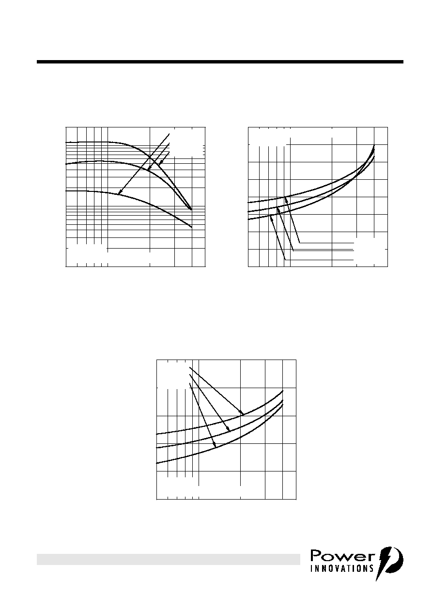
TYPICAL CHARACTERISTICS
Figure 1.
Figure 2.
Figure 3.
TYPICAL DC CURRENT GAIN
vs
COLLECTOR CURRENT
I
C
- Collector Current - A
0∑5
5∑0
1∑0
h
FE
- Typical DC Current Gain
20000
100
1000
10000
TCS110AD
T
C
= -40∞C
T
C
= 25∞C
T
C
= 100∞C
V
CE
= 3 V
t
p
= 300 µs, duty cycle < 2%
COLLECTOR-EMITTER SATURATION VOLTAGE
vs
COLLECTOR CURRENT
I
C
- Collector Current - A
0∑5
5∑0
1∑0
V
CE(sat)
- Collector-Emitter Saturation Voltage - V
0
0∑5
1∑0
1∑5
2∑0
TCS110AB
T
C
= -40∞C
T
C
= 25∞C
T
C
= 100∞C
t
p
= 300 µs, duty cycle < 2%
I
B
= I
C
/ 100
BASE-EMITTER SATURATION VOLTAGE
vs
COLLECTOR CURRENT
I
C
- Collector Current - A
0∑5
5∑0
1∑0
V
BE(sat)
- Base-Emitter Saturation Voltage - V
0∑5
1∑0
1∑5
2∑0
2∑5
3∑0
TCS110AC
T
C
= -40∞C
T
C
= 25∞C
T
C
= 100∞C
I
B
= I
C
/ 100
t
p
= 300 µs, duty cycle < 2%
BDW53, BDW53A, BDW53B, BDW53C, BDW53D
NPN SILICON POWER DARLINGTONS
4
AUGUST 1978 - REVISED MARCH 1997
P R O D U C T I N F O R M A T I O N
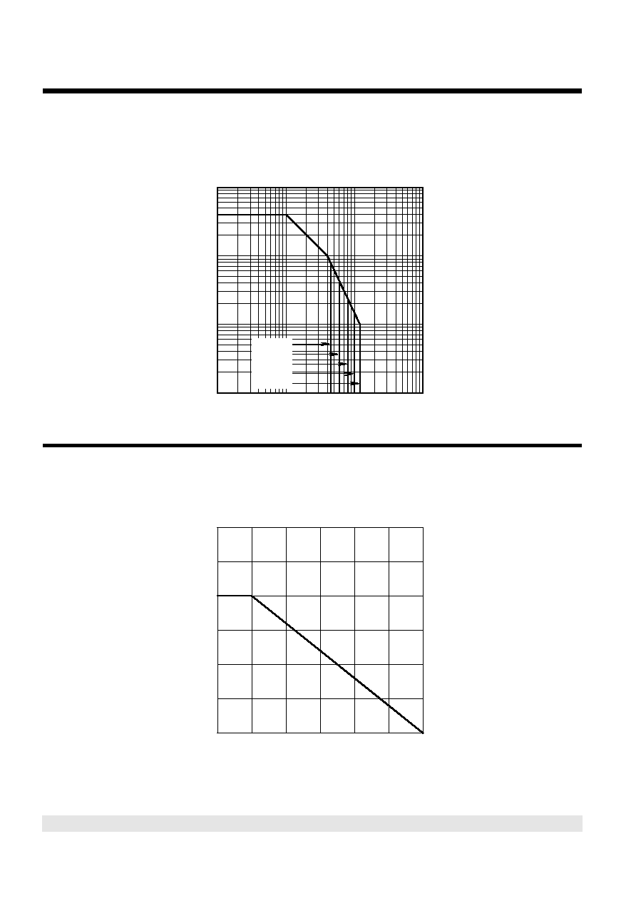
MAXIMUM SAFE OPERATING REGIONS
Figure 4.
THERMAL INFORMATION
Figure 5.
MAXIMUM FORWARD-BIAS
SAFE OPERATING AREA
V
CE
- Collector-Emitter Voltage - V
1∑0
10
100
1000
I
C
- Collector Current - A
0.01
0∑1
1∑0
10
SAS110AC
BDW53
BDW53A
BDW53B
BDW53C
BDW53D
MAXIMUM POWER DISSIPATION
vs
CASE TEMPERATURE
T
C
- Case Temperature - ∞C
0
25
50
75
100
125
150
P
tot
- Maximum Power Dissipation - W
0
10
20
30
40
50
60
TIS110AB
BDW53, BDW53A, BDW53B, BDW53C, BDW53D
NPN SILICON POWER DARLINGTONS
5
AUGUST 1978 - REVISED MARCH 1997
P R O D U C T I N F O R M A T I O N
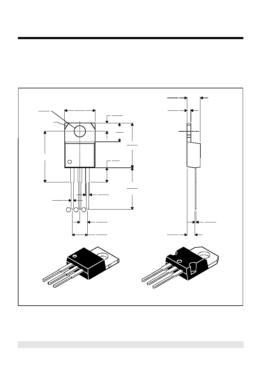
TO-220
3-pin plastic flange-mount package
This single-in-line package consists of a circuit mounted on a lead frame and encapsulated within a plastic
compound. The compound will withstand soldering temperature with no deformation, and circuit performance
characteristics will remain stable when operated in high humidity conditions. Leads require no additional
cleaning or processing when used in soldered assembly.
MECHANICAL DATA
TO220
ALL LINEAR DIMENSIONS IN MILLIMETERS
¯
1,23
1,32
4,20
4,70
1
2
3
0,97
0,61
see Note C
see Note B
10,0
10,4
2,54
2,95
6,0
6,6
14,55
15,90
12,7
14,1
3,5
6,1
1,07
1,70
2,34
2,74
4,88
5,28
3,71
3,96
0,41
0,64
2,40
2,90
VERSION 2
VERSION 1
NOTES: A. The centre pin is in electrical contact with the mounting tab.
B. Mounting tab corner profile according to package version.
C. Typical fixing hole centre stand off height according to package version.
Version 1, 18.0 mm. Version 2, 17.6 mm.
MDXXBE