 | –≠–ª–µ–∫—Ç—Ä–æ–Ω–Ω—ã–π –∫–æ–º–ø–æ–Ω–µ–Ω—Ç: BUL791 | –°–∫–∞—á–∞—Ç—å:  PDF PDF  ZIP ZIP |
BUL791
NPN SILICON POWER TRANSISTOR
P R O D U C T I N F O R M A T I O N
1
JULY 1991 - REVISED SEPTEMBER 1997
Copyright © 1997, Power Innovations Limited, UK
Information is current as of publication date. Products conform to specifications in accordance
with the terms of Power Innovations standard warranty. Production processing does not
necessarily include testing of all parameters.
q
Designed Specifically for High Frequency
Electronic Ballasts up to 125 W
q
h
FE
6 to 22 at V
CE
= 1 V, I
C
= 2 A
q
Low Power Losses (On-state and Switching)
q
Key Parameters Characterised at High
Temperature
q
Tight and Reproducible Parametric
Distributions
B
C
E
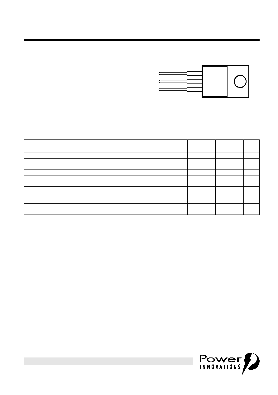
TO-220 PACKAGE
(TOP VIEW)
Pin 2 is in electrical contact with the mounting base.
MDTRACA
1
2
3
NOTES: 1. This value applies for t
p
= 10 ms, duty cycle
2%.
2. This value applies for t
p
= 300 µs, duty cycle
2%.
absolute maximum ratings at 25∞C ambient temperature (unless otherwise noted)
RATING
SYMBOL
VALUE
UNIT
Collector-emitter voltage (V
BE
= 0)
V
CES
700
V
Collector-base voltage (I
E
= 0)
V
CBO
700
V
Collector-emitter voltage (I
B
= 0)
V
CEO
400
V
Emitter-base voltage
V
EBO
9
V
Continuous collector current
I
C
4
A
Peak collector current (see Note 1)
I
CM
8
A
Peak collector current (see Note 2)
I
CM
14
A
Continuous base current
I
B
2.5
A
Peak base current (see Note 2)
I
BM
3.5
A
Continuous device dissipation at (or below) 25∞C case temperature
P
tot
75
W
Operating junction temperature range
T
j
-65 to +150
∞C
Storage temperature range
T
stg
-65 to +150
∞C

BUL791
NPN SILICON POWER TRANSISTOR
2
JULY 1991 - REVISED SEPTEMBER 1997
P R O D U C T I N F O R M A T I O N
NOTES: 3. Inductive loop switching measurement.
4. These parameters must be measured using pulse techniques, t
p
= 300 µs, duty cycle
2%.
5. These parameters must be measured using voltage-sensing contacts, separate from the current carrying contacts, and located
within 3.2 mm from the device body.
electrical characteristics at 25∞C case temperature (unless otherwise noted)
PARAMETER
TEST CONDITIONS
MIN
TYP
MAX
UNIT
V
CEO(sus)
Collector-emitter
sustaining voltage
I
C
= 100 mA
L = 25 mH
(see Note 3)
400
V
I
CES
Collector-emitter
cut-off current
V
CE
= 700 V
V
CE
= 700 V
V
BE
= 0
V
BE
= 0
T
C
= 90∞C
10
200
µA
I
EBO
Emitter cut-off
current
V
EB
= 9 V
I
C
= 0
1
mA
V
BE(sat)
Base-emitter
saturation voltage
I
B
= 400 mA
I
B
= 400 mA
I
C
= 2 A
I
C
= 2 A
(see Notes 4 and 5)
T
C
= 90∞C
0.94
0.86
1
V
V
CE(sat)
Collector-emitter
saturation voltage
I
B
= 400 mA
I
B
= 400 mA
I
C
= 2 A
I
C
= 2 A
(see Notes 4 and 5)
T
C
= 90∞C
0.25
0.3
0.4
V
h
FE
Forward current
transfer ratio
V
CE
= 1 V
V
CE
= 1 V
V
CE
= 5 V
I
C
= 10 mA
I
C
= 2 A
I
C
= 8 A
10
6
2
16.5
12
6.5
22
14
V
FCB
Collector-base forward
bias diode voltage
I
CB
= 60 mA
850
mV
thermal characteristics
PARAMETER
MIN
TYP
MAX
UNIT
R
JA
Junction to free air thermal resistance
62.5
∞C/W
R
JC
Junction to case thermal resistance
1.66
∞C/W
inductive-load switching characteristics at 25∞C case temperature
PARAMETER
TEST CONDITIONS
MIN
TYP
MAX
UNIT
t
sv
Storage time
I
C
= 2 A
L = 1 mH
I
B(on)
= 400 mA
I
B(off)
= 800 mA
V
CC
= 40 V
V
CLAMP
= 300 V
2.2
3
µs
t
fi
Current fall time
95
180
ns
t
xo
Cross over time
210
300
ns
t
sv
Storage time
I
C
= 2 A
L = 1 mH
I
B(on)
= 400 mA
I
B(off)
= 250 mA
V
CC
= 40 V
V
CLAMP
= 300 V
4
6
µs
t
fi
Current fall time
120
230
ns
resistive-load switching characteristics at 25∞C case temperature
PARAMETER
TEST CONDITIONS
MIN
TYP
MAX
UNIT
t
sv
Storage time
I
C
= 2 A
V
CC
= 300 V
I
B(on)
= 400 mA
I
B(off)
= 400 mA
2.2
3
µs
t
fi
Current fall time
160
250
ns

3
JULY 1991 - REVISED SEPTEMBER 1997
BUL791
NPN SILICON POWER TRANSISTOR
P R O D U C T I N F O R M A T I O N
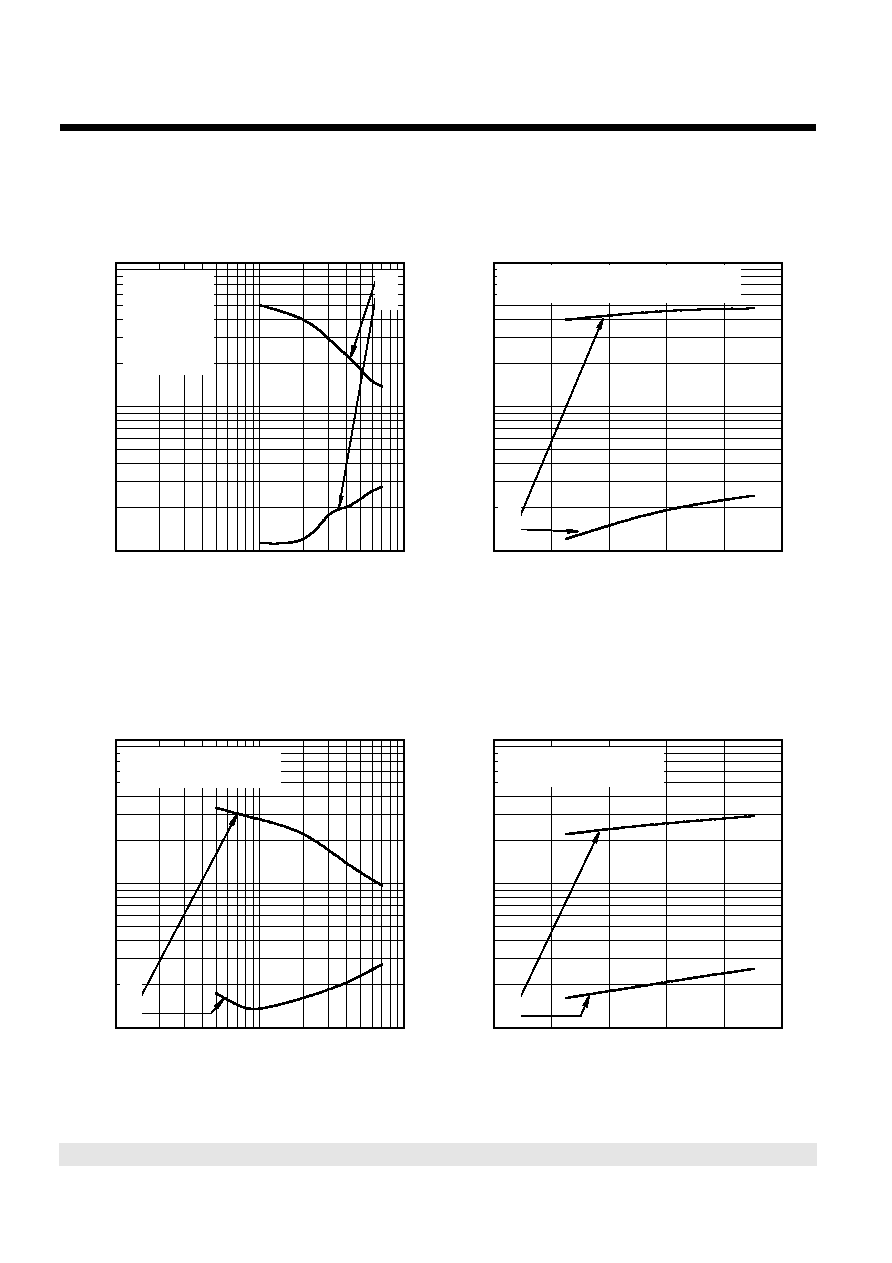
TYPICAL CHARACTERISTICS
Figure 1.
Figure 2.
Figure 3.
Figure 4.
FORWARD CURRENT TRANSFER RATIO
vs
COLLECTOR CURRENT
I
C
- Collector Current - A
20
0∑01
0∑1
1∑0
10
h
FE
- Forward Current Transfer Ratio
30
1∑0
10
L791CHF
T
C
= 25∞C
V
CE
= 1 V
V
CE
= 5 V
COLLECTOR-EMITTER SATURATION VOLTAGE
vs
COLLECTOR CURRENT
I
C
- Collector Current - A
0∑1
1∑0
10
V
CE(sat)
- Collector-Emitter Saturation Voltage - V
0∑01
0∑1
1∑0
10
L791CVB
I
B
= I
C
/ 5
T
C
= 25∞C
T
C
= 90∞C
INDUCTIVE SWITCHING TIMES
vs
COLLECTOR CURRENT
I
C
- Collector Current - A
0∑1
1∑0
10
Inductive Switching Time - µs
0∑01
0∑1
1∑0
10
L791CI1
t
sv
t
xo
t
fi
I
B(on)
= I
C
/ 5
I
B(off)
= I
C
/ 2.5
V
CC
= 40 V
V
CLAMP
= 300 V
L = 1 mH
T
C
= 25∞C
INDUCTIVE SWITCHING TIMES
vs
CASE TEMPERATURE
T
C
- Case Temperature - ∞C
0
20
40
60
80
100
Inductive Switching Time - µs
0∑01
0∑1
1∑0
10
L791CI3
t
sv
t
fi
I
B(on)
= 400 mA, V
CC
= 40 V, L
= 1 mH
I
B(off)
= 800 mA, V
CLAMP
= 300 V, I
C
= 2 A
BUL791
NPN SILICON POWER TRANSISTOR
4
JULY 1991 - REVISED SEPTEMBER 1997
P R O D U C T I N F O R M A T I O N
TYPICAL CHARACTERISTICS
Figure 5.
Figure 6.
Figure 7.
Figure 8.
INDUCTIVE SWITCHING TIMES
vs
COLLECTOR CURRENT
I
C
- Collector Current - A
0∑1
1∑0
10
Inductive Switching Time - µs
0∑1
1∑0
10
L791CI2
t
sv
t
fi
I
B(on)
= I
C
/ 5
I
B(off)
= I
C
/ 8
V
CC
= 40 V
V
CLAMP
= 300 V
L = 1 mH
T
C
= 25∞C
INDUCTIVE SWITCHING TIMES
vs
CASE TEMPERATURE
T
C
- Case Temperature - ∞C
0
20
40
60
80
100
Inductive Switching Time - µs
0∑1
1∑0
10
L791CI4
t
sv
t
fi
I
B(on)
= 400 mA, V
CC
= 40 V, L = 1 mH
I
B(off)
= 250 mA, V
CLAMP
= 300 V, I
C
= 2 A
RESISTIVE SWITCHING TIMES
vs
COLLECTOR CURRENT
I
C
- Collector Current - A
0∑1
1∑0
10
Resistive Switching Time - µs
0∑1
1∑0
10
L791CR1
I
B(on)
= I
C
/ 5, V
CC
= 300 V
I
B(off)
= I
C
/ 5, T
C
= 25∞C
t
sv
t
fi
RESISTIVE SWITCHING TIMES
vs
CASE TEMPERATURE
T
C
- Case Temperature - ∞C
0
20
40
60
80
100
Resistive Switching Time - µs
0∑1
1∑0
10
L791CR2
t
sv
t
fi
I
B(on)
= 400 mA, V
CC
= 300 V
I
B(off)
= 400 mA, I
C
= 2 A
5
JULY 1991 - REVISED SEPTEMBER 1997
BUL791
NPN SILICON POWER TRANSISTOR
P R O D U C T I N F O R M A T I O N
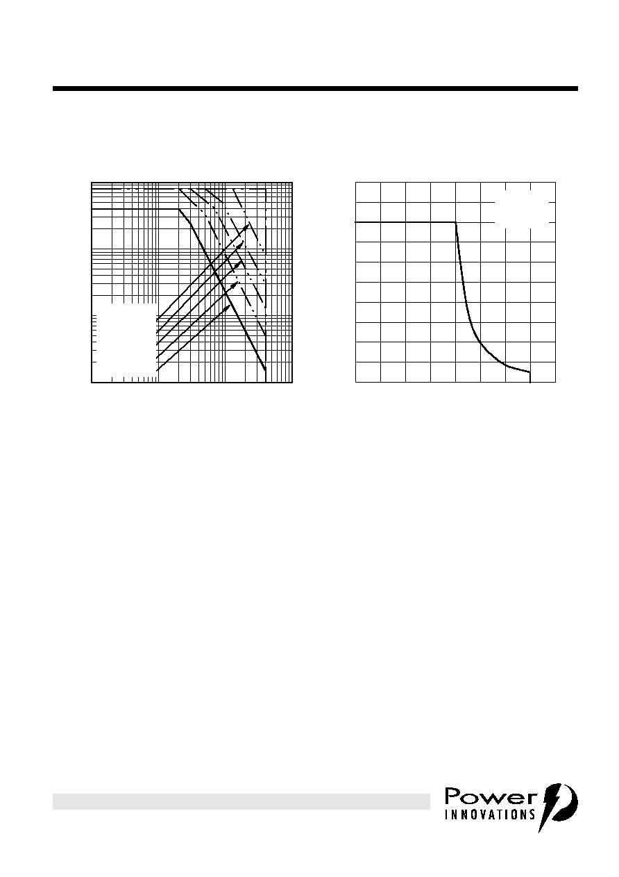
MAXIMUM SAFE OPERATING REGIONS
Figure 9.
Figure 10.
MAXIMUM FORWARD-BIAS
SAFE OPERATING AREA
V
CE
- Collector-Emitter Voltage - V
1∑0
10
100
1000
I
C
- Collector Current - A
0∑01
0∑1
1∑0
10
L791CFB
T
C
= 25∞C
t
p
= 10 µs
t
p
= 100 µs
t
p
= 1 ms
t
p
= 10 ms
DC Operation
MAXIMUM REVERSE-BIAS
SAFE OPERATING AREA
V
CE
- Collector-Emitter Voltage - V
0
100
200
300
400
500
600
700
800
I
C
- Collector Current - A
0
2
4
6
8
10
L791CRB
I
B(on)
= I
C
/ 5
V
BE(off)
= -5 V
T
C
= 25∞C