 | –≠–ª–µ–∫—Ç—Ä–æ–Ω–Ω—ã–π –∫–æ–º–ø–æ–Ω–µ–Ω—Ç: BULD50KC | –°–∫–∞—á–∞—Ç—å:  PDF PDF  ZIP ZIP |
BULD50KC, BULD50SL
NPN SILICON TRANSISTOR WITH INTEGRATED DIODE
P R O D U C T I N F O R M A T I O N
1
FEBRUARY 1994 - REVISED SEPTEMBER 1997
Copyright © 1997, Power Innovations Limited, UK
Information is current as of publication date. Products conform to specifications in accordance
with the terms of Power Innovations standard warranty. Production processing does not
necessarily include testing of all parameters.
q
Designed Specifically for High Frequency
Electronic Ballasts
q
Integrated Fast t
rr
Anti-Parallel Diode,
Enhancing Reliability
q
Diode t
rr
Typically 1 µs
q
New Low-Height SL Power Package,
TO220 Pin-Compatible
q
Tightly Controlled Transistor Storage Times
q
Voltage Matched Integrated Transistor and
Diode
q
Characteristics Optimised for Cool Running
q
Diode-Transistor Charge Coupling
Minimised to Enhance Frequency Stability
description
The new BULDxx range of transistors have been
designed specifically for use in High Frequency
Electronic Ballasts (HFEB's). This range of
switching transistors has tightly controlled
storage times and an integrated fast t
rr
anti-
parallel diode. The revolutionary design ensures
that the diode has both fast forward and reverse
recovery times, achieving the same performance
as a discrete anti-parallel diode plus transistor.
The integrated diode has minimal charge
coupling with the transistor, increasing frequency
stability, especially in lower power circuits where
the circulating currents are low. By design, this
new device offers a voltage matched integrated
transistor and anti-parallel diode.
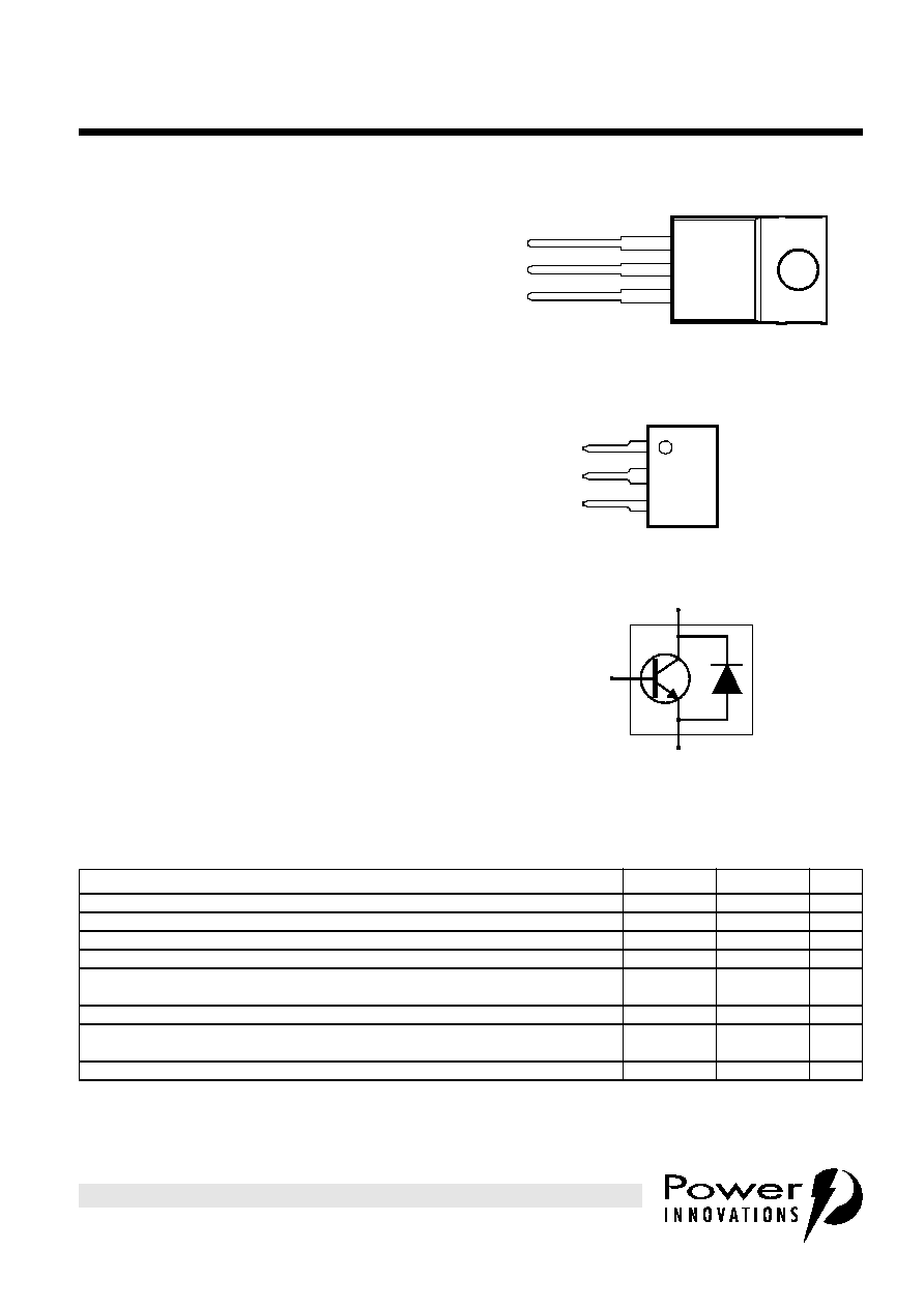
device symbol
B
C
E
TO-220 PACKAGE
(TOP VIEW)
Pin 2 is in electrical contact with the mounting base.
MDTRACA
1
2
3
1
2
3
B
C
E
SL PACKAGE
(TOP VIEW)
B
C
E
absolute maximum ratings at 25∞C
(unless otherwise noted)
RATING
SYMBOL
VALUE
UNIT
Collector-emitter voltage (V
BE
= 0)
V
CES
600
V
Collector-base voltage (I
E
= 0)
V
CBO
600
V
Collector-emitter voltage (I
B
= 0)
V
CEO
400
V
Emitter-base voltage
V
EBO
9
V
Continuous collector current
BULD50KC
BULD50SL (see Note 1)
I
C
3.5
A
Peak collector current (see Note 2)
I
CM
6
A
Continuous base current
BULD50KC
BULD50SL (see Note 1)
I
B
1.5
A
Peak base current (see Note 2)
I
BM
2.5
A
NOTES: 1. This value applies for t
p
=
1 s.
2. This value applies for t
p
=
10 ms, duty cycle
2%.
25∞C case temperature for BULD50KC, and
25∞C ambient temperature for BULD50SL

BULD50KC, BULD50SL
NPN SILICON TRANSISTOR WITH INTEGRATED DIODE
2
FEBRUARY 1994 - REVISED SEPTEMBER 1997
P R O D U C T I N F O R M A T I O N
NOTES: 3. These parameters must be measured using pulse techniques, t
p
= 300 µs, duty cycle
2%.
4. These parameters must be measured using voltage-sensing contacts, separate from the current carrying contacts, and located
within 3.2 mm from the device body.
5. Tested in a typical High Frequency Electronic Ballast.
RATING
SYMBOL
VALUE
UNIT
Continuous device dissipation
BULD50KC
BULD50SL
P
tot
50
see Figure 11
W
Maximum average continuous diode forward current
I
E(av)
0.5
A
Operating junction temperature range
T
j
-65 to +150
∞C
Storage temperature range
T
stg
-65 to +150
∞C
electrical characteristics at 25∞C case temperature
PARAMETER
TEST CONDITIONS
MIN
TYP
MAX
UNIT
V
CEO(sus)
Collector-emitter
sustaining voltage
I
C
= 100 mA
L = 25 mH
400
V
I
CES
Collector-emitter
cut-off current
V
CE
= 600 V
V
BE
= 0
10
µA
I
EBO
Emitter cut-off
current
V
EB
= 9 V
I
C
= 0
1
mA
V
BE(sat)
Base-emitter
saturation voltage
I
B
= 150 mA
I
C
= 750 mA
(see Notes 3 and 4)
0.9
1.1
V
V
CE(sat)
Collector-emitter
saturation voltage
I
B
= 150 mA
I
B
= 300 mA
I
C
= 750 mA
I
C
= 1.5 A
(see Notes 3 and 4)
0.2
0.4
0.5
1
V
h
FE
Forward current
transfer ratio
V
CE
= 10 V
V
CE
= 1 V
V
CE
= 5 V
I
C
= 10 mA
I
C
= 750 mA
I
C
= 1.5 A
(see Notes 3 and 4)
10
10
10
17
15
15
20
20
V
EC
Anti-parallel diode
forward voltage
I
E
= 1 A
(see Notes 3 and 4)
1.25
1.5
V
t
rr
Anti-parallel diode
reverse recovery time
(see Note 5)
1
µs
thermal characteristics
PARAMETER
MIN
TYP
MAX
UNIT
R
JA
Junction to free air thermal resistance
BULD50KC
BULD50SL
62.5
115
∞C/W
R
JC
Junction to case thermal resistance
BULD50KC
2.5
∞C/W
inductive-load switching characteristics at 25∞C case temperature
PARAMETER
TEST CONDITIONS
MIN
TYP
MAX
UNIT
t
sv
Storage time
I
C
= 750 mA
L = 1 mH
I
B(on)
= 150 mA
I
B(off)
= 150 mA
V
CC
= 40 V
V
CLAMP
= 300 V
3.35
4.5
µs
resistive-load switching characteristics at 25∞C case temperature
PARAMETER
TEST CONDITIONS
MIN
TYP
MAX
UNIT
t
fi
Current fall time
I
C
= 750 mA
V
CC
= 300 V
I
B(on)
= 150 mA
I
B(off)
= 150 mA
150
250
ns
absolute maximum ratings at 25∞C
(unless otherwise noted) (continued)

3
FEBRUARY 1994 - REVISED SEPTEMBER 1997
BULD50KC, BULD50SL
NPN SILICON TRANSISTOR WITH INTEGRATED DIODE
P R O D U C T I N F O R M A T I O N
TYPICAL CHARACTERISTICS
Figure 1.
Figure 2.
Figure 3.
FORWARD CURRENT TRANSFER RATIO
vs
COLLECTOR CURRENT
I
C
- Collector Current - A
0∑01
0∑1
1∑0
10
h
FE
- Forward Current Transfer Ratio
30
1∑0
10
LDX50SHF
V
CE
= 1 V
V
CE
= 5 V
V
CE
= 10 V
T
C
= 25∞C
ANTI-PARALLEL DIODE
INSTANTANEOUS FORWARD CURRENT
vs
INSTANTANEOUS FORWARD VOLTAGE
V
EC
- Instantaneous Forward Voltage - V
0
0∑5
1∑0
1∑5
2∑0
2∑5
3∑0
I
E
- Instantaneous Forward Current - A
0∑01
0∑1
1∑0
10
LDX50SVF
T
C
= 25∞C
BASE-EMITTER SATURATION VOLTAGE
vs
CASE TEMPERATURE
T
C
- Case Temperature - ∞C
0
25
50
75
100
V
BE(sat)
- Base-Emitter Saturation Voltage - V
0.6
0.7
0.8
0.9
1.0
LDX50SVB
I
C
= 750 mA
I
B
= 150 mA

BULD50KC, BULD50SL
NPN SILICON TRANSISTOR WITH INTEGRATED DIODE
4
FEBRUARY 1994 - REVISED SEPTEMBER 1997
P R O D U C T I N F O R M A T I O N
MAXIMUM SAFE OPERATING REGIONS
Figure 4.
Figure 5.
Figure 6.
MAXIMUM FORWARD-BIAS
SAFE OPERATING AREA
V
CE
- Collector-Emitter Voltage - V
1∑0
10
100
1000
I
C
- Collector Current - A
0∑01
0∑1
1∑0
10
LDX50CFB
BULD50KC
T
C
= 25∞C
t
p
= 100 µs
t
p
= 1 ms
t
p
= 10 ms
DC Operation
MAXIMUM FORWARD-BIAS
SAFE OPERATING AREA
V
CE
- Collector-Emitter Voltage - V
1∑0
10
100
1000
I
C
- Collector Current - A
0∑01
0∑1
1∑0
10
LDX50SFB
BULD50SL
T
A
= 25∞C
t
p
= 100 µs
t
p
= 10 ms
t
p
= 1 s
MAXIMUM REVERSE-BIAS
SAFE OPERATING AREA
V
CE
- Collector-Emitter Voltage - V
0
100
200
300
400
500
600
700
800
I
C
- Collector Current - A
0
2
4
6
8
LDX50SRB
I
B(on)
= I
C
/ 5
V
BE(off)
= -5 V
T
A
= 25∞C

5
FEBRUARY 1994 - REVISED SEPTEMBER 1997
BULD50KC, BULD50SL
NPN SILICON TRANSISTOR WITH INTEGRATED DIODE
P R O D U C T I N F O R M A T I O N
THERMAL INFORMATION
Figure 7.
Figure 8.
THERMAL RESPONSE JUNCTION TO AMBIENT
vs
POWER PULSE DURATION
t1 - Power Pulse Duration - s
10
-4
10
-3
10
-2
10
-1
10
0
10
1
10
2
10
3
Z
JA
/R
JA
- Normalised Transient Thermal Impedance
0∑001
0∑01
0∑1
1∑0
LDX50CZA
40%
60%
20%
10%
0%
BULD50KC
T
A
= 25∞C
T
J max
(
)
T
A
P
D peak
(
)
Z
J A
R
J A
R
JA max
(
)
∑
∑
=
≠
t1
t2
duty cycle = t1/t2
Read time at end of t1,
THERMAL RESPONSE JUNCTION TO AMBIENT
vs
POWER PULSE DURATION
t1 - Power Pulse Duration - s
10
-4
10
-3
10
-2
10
-1
10
0
10
1
10
2
10
3
Z
JA
/R
JA
- Normalised Transient Thermal Impedance
0∑001
0∑01
0∑1
LDX50SZA
40%
60%
20%
10%
0%
BULD50SL
T
A
= 25∞C
T
J max
(
)
T
A
P
D peak
(
)
Z
J A
R
J A
R
JA max
(
)
∑
∑
=
≠
t1
t2
duty cycle = t1/t2
Read time at end of t1,