 | –≠–ª–µ–∫—Ç—Ä–æ–Ω–Ω—ã–π –∫–æ–º–ø–æ–Ω–µ–Ω—Ç: R3612 | –°–∫–∞—á–∞—Ç—å:  PDF PDF  ZIP ZIP |

R3612
PROGRAMMABLE OVERVOLTAGE PROTECTOR
FOR ERICSSON COMPONENTS 3357/3 DCLIC
P R O D U C T I N F O R M A T I O N
1
DECEMBER 1995 - REVISED SEPTEMBER 1997
Copyright © 1997, Power Innovations Limited, UK
Information is current as of publication date. Products conform to specifications in accordance
with the terms of Power Innovations standard warranty. Production processing does not
necessarily include testing of all parameters.
OVERVOLTAGE PROTECTION FOR ERICSSON COMPONENTS LINE INTERFACE CIRCUITS
q
PBA 3357/3 DCLIC Overvoltage Protector
q
Dual Voltage-Programmable Protector
- Wide 0 to -70 V Programming Range
- Low Voltage Overshoot Crowbar and Diode
- Low 5 mA max. Triggering Current
- Does not Charge Gate Supply
- Specified for 0∞C to 70∞C Operation
- Plastic Dual-in-line Package
q
Rated for International Surge Wave Shapes
description
The R3612 is a dual forward-conducting buffered
p-gate over voltage protector in a plastic DIP
package. It is designed to protect the Ericsson
Components PBA 3357/3 DCLIC (Dual Channel
Complete Line Interface Circuit) against over
voltages on the telephone line caused by
lightning, a.c. power contact and induction. The
R3612 limits voltages that exceed the DCLIC
supply rail voltage.
The DCLIC line driver section is powered from
0 V (ground) and a negative voltage in the region
of -44 V to -56 V. The protector gate is connected
to this negative supply. This references the
protection (clipping) voltage to the negative
supply voltage. As the protection voltage will
track the negative supply voltage the over
voltage stress on the DCLIC is minimised.
Positive over voltages are clipped to ground by a
low voltage overshoot diode. Negative over
voltages are initially clipped close to the DCLIC
negative supply rail value. If sufficient current is
available from the over voltage, then the
protector will crowbar into a low voltage on-state
condition. As the over voltage subsides the high
holding current of the crowbar prevents d.c.
latchup.
The buffered gate design reduces the loading on
the DCLIC supply during over voltages caused
WAVE SHAPE
STANDARD
I
TSP
A
2/10 µs
TR-NWT-001089
80
0.5/700 µs
RLM88
38
10/700 µs
K17, K20, K21
38
10/1000 µs
TR-NWT-001089
30
by power cross and induction. The gate
characteristic is designed to produce a net
current drain on the interface circuit voltage
supply during low level power cross or induction.
This removes the need for a separate clamping
diode across the voltage supply.
These monolithic protection devices are
fabricated in ion-implanted planar vertical power
structures for high reliability and in normal
system operation they are virtually transparent.
Characteristic values for the R3612 are
measured either at the extremes of the DCLIC
recommended operating voltage range (-44 V to
-56 V) or at the DCLIC maximum rated supply
voltage (-70 V).
device symbol
Terminals K1, K2 and A correspond to the alternative
line designators of T, R and G or A, B and C. The
negative protection voltage is controlled by the voltage,
V
GG,
applied to the G terminal.
SD6XAE
A
K1
G
K2
MD6XAV
P PACKAGE
(TOP VIEW)
NC - No internal connection
Terminal typical application names shown in
parenthesis
1
2
3
4
5
6
7
8
K2
G
K1
NC
K1
A
A
K2
(Tip)
(Ground)
(Ground)
(Ring)
(Gate)
(Tip)
(Ring)

R3612
PROGRAMMABLE OVERVOLTAGE PROTECTOR
FOR ERICSSON COMPONENTS 3357/3 DCLIC
2
DECEMBER 1995 - REVISED SEPTEMBER 1997
P R O D U C T I N F O R M A T I O N
absolute maximum ratings
NOTES: 1. Initially the protector must be in thermal equilibrium with 0∞C
T
J
70∞C. The surge may be repeated after the device returns to its
initial conditions.
2. Above 70∞C, derate linearly to zero at 150∞C lead temperature.
RATING
SYMBOL
VALUE
UNIT
Non-repetitive peak off-state voltage, I
G
= 0, 0∞C
T
J
70∞C
V
DSM
-90
V
Repetitive peak off-state voltage, I
G
= 0, 0∞C
T
J
70∞C
V
DRM
-80
V
Repetitive peak gate-cathode voltage, V
KA
= 0, 0∞C
T
J
70∞C
V
GKRM
-80
V
Non-repetitive peak on-state pulse current (see Notes 1 and 2)
I
TSP
A
10/1000 µs (Bellcore TR-NWT-001089, Section 4 and Appendix A)
30
0.2/310 µs (RLM88, open-circuit voltage wave shape 1.5 kV 0.5/700 µs)
5/310 µs (CCITT K17, K20 & K21, open-circuit voltage wave shape 1.5 kV 10/700 µs))
38
38
2/10 µs (Bellcore TR-NWT-001089, Section 4 and Appendix A)
80
Non-repetitive peak on-state current, 50 Hz (see Notes 1 and 2)
I
TSM
A
200 ms
5.6
1 s
25 s
900 s
3.5
0.7
0.42
Non-repetitive peak gate current, 1/2 µs,(see Notes 1 and 2)
I
GSM
25
A
Junction temperature
T
J
-55 to +150
∞C
Storage temperature range
T
stg
-55 to +150
∞C
recommended operating conditions
MIN
TYP
MAX
UNIT
C
G
Gate decoupling capacitor
220
nF
electrical characteristics, T
amb
= 25∞C (unless otherwise noted)
PARAMETER
TEST CONDITIONS
MIN
TYP
MAX
UNIT
I
D
Off-state current
V
D
= V
DRM
, V
GK
= 0
T
J
= 0∞C
5
µA
T
J
= 70∞C
50
µA
V
(BO)
Breakover voltage
I
T
= 20 A, I3124 generator, open-circuit voltage wave shape 1 5 kV
0.5/700 µs, board resistance R
S
= 35
, C
G
= 220 nF, V
GG
= -56 V
(See Note 3 and Figure 1.)
-80
V
t
(BR)
Breakdown time
I
T
= 20 A, I3124 generator, open-circuit voltage
wave shape 1 5 kV 0.5/700 µs, board resist-
ance R
S
= 35
, C
G
= 220 nF, V
GG
= -56 V
(See Note 3 and Figure 1.)
V
(BR)
< -70 V
V
(BR)
< -58.5 V
1
10000
µs
V
F
Forward voltage
I
F
= 5 A, t
w
= 500 µs
3
V
V
FRM
Peak forward recovery
voltage
I
F
= 20 A,I3124 generator, open-circuit voltage wave shape 1 5 kV
0.5/700 µs, board resistance R
S
= 35
, C
G
= 220 nF, V
GG
= -56 V
(See Note 4 and Figure 1.)
15
V
t
FRM
Forward recovery time
I
T
= 20 A, I3124 generator, open-circuit voltage
wave shape 1 5 kV 0.5/700 µs, board resist-
ance R
S
= 35
, C
G
= 220 nF, V
GG
= -56 V
(See Note 4 and Figure 1.)
V
F
> 10 V
V
F
> 5 V
V
F
> 1 V
0.25
1
10000
µs
I
H
Holding current
I
T
= 1 A, di/dt = -1A/ms, V
GG
= -70 V, 0∞C
T
J
70∞C
105
mA
I
GAS
Gate reverse current
V
GG
= -70 V, V
AK
= 0
T
J
= 0∞C
-5
µA
T
J
= 70∞C
-50
I
GAT
Gate reverse current,
on state
I
T
= 0.5 A, t
w
= 500 µs, V
GG
= -70 V
-1
mA

3
DECEMBER 1995 - REVISED SEPTEMBER 1997
R3612
PROGRAMMABLE OVERVOLTAGE PROTECTOR
FOR ERICSSON COMPONENTS 3357/3 DCLIC
P R O D U C T I N F O R M A T I O N
NOTES:
3.PBA 3357/3 maximum negative voltage pulse rating is -120 V for 0.25 µs, -90 V for 1 µs, -70 V for 10 ms and -70 V for d.c.
Compliance to these conditions is guaranteed by the maximum breakover voltage and the breakdown times of the R3612.
4.PBA 3357/3 maximum positive voltage pulse rating is 15 V for 0.25 µs, 10 V for 1 µs, 5 V for 10 ms and 1 V for d.c.. Compliance
to these conditions is guaranteed by the peak forward recovery voltage and the forward recovery times of the R3612
5. These capacitance measurements employ a three terminal capacitance bridge incorporating a guard circuit. The unmeasured
device terminals are a.c. connected to the guard terminal of the bridge.
PARAMETER
TEST CONDITIONS
MIN
TYP
MAX
UNIT
I
GAF
Gate reverse current,
forward conducting
state
I
F
= 1 A, t
w
= 500 µs, V
GG
= -70 V
-10
mA
I
GT
Gate trigger current
I
T
= 5 A, t
p(g)
20 µs, V
GG
= -44 V
5
mA
V
GT
Gate trigger voltage
I
T
= 5 A, t
p(g)
20 µs, V
GG
= -44 V
2.5
V
C
AK
Anode-cathode off-
state capacitance
f = 1 MHz, V
d
= 1 V, I
G
= 0, (see Note 5)
V
D
= -3 V
110
pF
V
D
= -56 V
60
thermal characteristics
PARAMETER
TEST CONDITIONS
MIN
TYP
MAX
UNIT
R
JA
Junction to free air thermal resistance
P
tot
= 0.8 W, T
A
= 25∞C, 5 cm
2
, FR4 PCB
100
∞C/W
PARAMETER MEASUREMENT INFORMATION
Figure 1. TRANSIENT LIMITS FOR R3612 LIMITING VOLTAGE
electrical characteristics, T
amb
= 25∞C (unless otherwise noted) (Continued)
10 ms
1 µs
0.25 µs
PBA 3357/3 DCLIC RING AND TIP VOLTAGE WITHSTAND
vs
TIME
0
5
10
15
VOLTAGE - V
-120
-110
-100
-90
-80
-70
0.25 µs
1 µs
Time

R3612
PROGRAMMABLE OVERVOLTAGE PROTECTOR
FOR ERICSSON COMPONENTS 3357/3 DCLIC
4
DECEMBER 1995 - REVISED SEPTEMBER 1997
P R O D U C T I N F O R M A T I O N
PARAMETER MEASUREMENT INFORMATION
Figure 2. VOLTAGE-CURRENT CHARACTERISTIC
THERMAL INFORMATION
Figure 3.
-v
I
S
V
S
V
GG
V
D
I
H
I
T
V
T
I
TSM
I
TSP
V
(BO)
I
(BO)
I
D
Quadrant I
Forward
Conduction
Characteristic
+v
+i
I
F
V
F
I
TSM
I
TSP
-i
Quadrant III
Switching
Characteristic
PM6XAA
V
GK(BO)
MAXIMUM NON-RECURRING 50 Hz CURRENT
t - Current Duration - s
0∑1
1
10
100
1000
I
TSM
- Maximum Non-Recurrent 50 Hz Current - A
0.1
1
10
vs
CURRENT DURATION
R3612
V
GEN
= 250 Vrms
R
GEN
= 10 to 150

5
DECEMBER 1995 - REVISED SEPTEMBER 1997
R3612
PROGRAMMABLE OVERVOLTAGE PROTECTOR
FOR ERICSSON COMPONENTS 3357/3 DCLIC
P R O D U C T I N F O R M A T I O N
DEVICE PARAMETERS
general
Thyristor based over voltage protectors, for telecommunications equipment, became popular in the late
1970s. These were fixed voltage breakover triggered devices, likened to solid state gas discharge tubes. As
these were new forms of thyristor, the existing thyristor terminology did not cover their special characteristics.
This resulted in the invention of new terms based on the application usage and device characteristic. Initially,
there was a wide diversity of terms to describe the same thing, but today the number of terms have reduced
and stabilised. Information on fixed voltage over voltage protector terms, symbols and their definitions is given
in the publication SLPDE05, "Over-voltage Protection For Telecommunication Systems - Data Manual and
Application Information", pp 1-4 to 1-6, Texas Instruments Limited, Bedford, 1994.
Programmable, (gated), over voltage protectors are relatively new and require additional parameters to
specify their operation. Similarly to the fixed voltage protectors, the introduction of these devices has resulted
in a wide diversity of terms to describe the same thing. This section has a list of alternative terms and the
parameter definitions used for this data sheet. In general, the Texas Instruments approach is to use terms
related to the device internal structure, rather than its application usage as a single device may have many
applications each using a different terminology for circuit connection.
terms, definitions and symbols
Thyristor over voltage protectors have substantially different characteristics and usage to the type of thyristor
covered by IEC 747-6. These differences necessitate the modification of some characteristic descriptions and
the introduction of new terms. Where possible terms are used from the following standards.
IEC 747-1:1983, Semiconductor devices - Discrete devices and integrated circuits - Part 1: General
IEC 747-2:1983, Semiconductor devices - Discrete devices and integrated circuits - Part 2: Rectifier Diodes
IEC 747-6:1983, Semiconductor devices - Discrete devices and integrated circuits - Part 6: Thyristors
main terminal ratings
Repetitive Peak Off-State Voltage, V
DRM
Rated maximum (peak) instantaneous voltage that may be applied in the off-state conditions including all d.c.
and repetitive voltage components.
Repetitive Peak On-State Current, I
TRM
Rated maximum (peak) value of a.c. power frequency on-state current of specified waveshape and frequency
which may be applied continuously.
Non-Repetitive Peak On-State Current, I
TSM
Rated maximum (peak) value of a.c. power frequency on-state surge current of specified waveshape and
frequency which may be applied for a specified time or number of a.c. cycles.
Non-Repetitive Peak Pulse Current, I
TSP
Rated maximum value of peak impulse pulse current of specified amplitude and waveshape that may be
applied.
Non-Repetitive Peak Forward Current, I
FSM
Rated maximum (peak) value of a.c. power frequency forward surge current of specified waveshape and
frequency which may be applied for a specified time or number of a.c. cycles.

R3612
PROGRAMMABLE OVERVOLTAGE PROTECTOR
FOR ERICSSON COMPONENTS 3357/3 DCLIC
6
DECEMBER 1995 - REVISED SEPTEMBER 1997
P R O D U C T I N F O R M A T I O N
Repetitive Peak Forward Current, I
FRM
Rated maximum (peak) value of a.c. power frequency forward current of specified waveshape and frequency
which may be applied continuously.
Critical rate of rise of on-state current, di/dt, (di
T
/dt)cr
Rated value of the rate of rise of current which the device can withstand without damage.
main terminal characteristics
Off-State Voltage, V
D
The d.c. voltage when the device is in the off-state.
Off-State Current, I
D
The d.c. value of current that results from the application of the off-state voltage, V
D
.
Repetitive Peak Off-State Current, I
DRM
The maximum (peak) value of off-state current that results from the application of the repetitive peak off-state
voltage, V
DRM
.
Breakover Voltage, V
(BO)
The maximum voltage across the device in or at the breakdown region measured under specified voltage rate
of rise and current rate of rise.
NOTE - Where a breakdown characteristic has several V
(BO)
values that need to be referenced, a numeric
suffix can be added and the relevant part of the breakdown current range specified (e.g. V
(BO)1
,
0 < I
(BR)
< 10 mA).
Holding Current, I
H
The minimum current required to maintain the device in the on-state.
Off-State Capacitance, C
O
, C
J
The capacitance in the off-state measured at specified frequency, f, amplitude, V
d
, and d.c. bias, V
D
.
Peak Forward Recovery Voltage, V
FRM
The maximum value of forward conduction voltage across the device upon the application of a specified
voltage rate of rise and current rate of rise following a zero or specified reverse-voltage condition.
Critical rate of rise of off-state voltage, dv/dt, (dv
D
/dt)cr
The maximum rate of rise of voltage (below V
DRM
) that will not cause switching from the off-state to the on-
state.
Breakover Current, I
(BO)
The instantaneous current flowing at the breakover voltage, V
(BO)
.
Switching Voltage, V
S
The instantaneous voltage across the device at the final point in the breakdown region prior to switching into
the on-state.
Switching Current, I
S
The instantaneous current flowing through the device at the switching voltage, V
S
.
On-State Voltage, V
T
The voltage across the device in the on-state condition at a specified current I
T
.

7
DECEMBER 1995 - REVISED SEPTEMBER 1997
R3612
PROGRAMMABLE OVERVOLTAGE PROTECTOR
FOR ERICSSON COMPONENTS 3357/3 DCLIC
P R O D U C T I N F O R M A T I O N
On-State Current, I
T
The current through the device in the on-state condition.
Forward Voltage, V
F
The voltage across the device in the forward conducting state at a specified current I
F
.
Forward Current, I
F
The current through the device in the forward conducting state.
thermal characteristics
Temperature Derating
Derating with temperature above a specified base temperature, expressed as a percentage, such as may be
applied to peak pulse current.
Thermal Resistance, R
JL
, R
JC
, R
JA
The effective temperature rise per unit power dissipation of a designated junction, above the temperature of a
stated external reference point (lead, case, or ambient) under conditions of thermal equilibrium.
Transient thermal impedance, Z
JL(t)
, Z
JC(t)
, Z
JA(t)
The change in the difference between the virtual junction temperature and the temperature of a specified
reference point or region (lead, case, or ambient) at the end of a time interval divided by the step function
change in power dissipation at the beginning of the same time interval which causes the change of
temperature-difference.
NOTE - It is the thermal impedance of the junction under conditions of change and is generally given in the
form of a curve as a function of the duration of an applied pulse.
(Virtual-)Junction Temperature, T
J
A theoretical temperature representing the temperature of the junction(s) calculated on the basis of a
simplified model of the thermal and electrical behaviour of the device.
Maximum Junction Temperature, T
JM
The maximum value of permissible junction temperature, due to self heating, which a TSS can withstand
without degradation.
gate terminal parameters
Gate Trigger Current, I
GT
The lowest gate current required to switch a device from the off state to the on state.
Gate Trigger Voltage, V
GT
The gate voltage required to produce the gate trigger current, I
GT
.
Gate-to-Adjacent Terminal Peak Off-State Voltage, V
GDM
The maximum gate to cathode voltage for a p-gate device or gate to anode voltage for an n-gate device that
may be applied such that a specified off-state current, I
D
, at a rated off-state voltage, V
D
, is not exceeded.
Peak Off-State Gate Current, I
GDM
The maximum gate current that results from the application of the peak off-state gate voltage, V
GDM
.
Gate Reverse Current, Adjacent Terminal Open, I
GAO ,
I
GKO
The current through the gate terminal when a specified gate bias voltage, V
G
, is applied and the cathode
terminal for a p-gate device or anode terminal for an n-gate device is open circuited.

R3612
PROGRAMMABLE OVERVOLTAGE PROTECTOR
FOR ERICSSON COMPONENTS 3357/3 DCLIC
8
DECEMBER 1995 - REVISED SEPTEMBER 1997
P R O D U C T I N F O R M A T I O N
Gate Reverse Current, Main Terminals Short Circuited, I
GAS
, I
GKS
The current through the gate terminal when a specified gate bias voltage, V
G
, is applied and the cathode
terminal for a p-gate device or anode terminal for an n-gate device is short-circuited to the third terminal.
NOTE-This definition only applies to devices with integrated series gate blocking diodes.
Gate Reverse Current, On-State, I
GAT
, I
GKT
The current through the gate terminal when a specified gate bias voltage, V
G
, is applied and a specified on-
state current, I
T
, is flowing.
NOTE-This definition only applies to devices with integrated series gate blocking diodes.
Gate Reverse Current, Forward Conducting State, I
GAF
, I
GKF
The current through the gate terminal when a specified gate bias voltage, V
G
, is applied and a specified
forward conduction current, I
F
, is flowing.
NOTE-This definition only applies to devices with integrated series gate blocking diodes.
Gate Switching Charge, Q
GS
The charge through the gate terminal, under impulse conditions, during the transition from the off-state to the
switching point, when a specified gate bias voltage, V
G
, is applied.
Peak Gate Switching Current, I
GSM
The maximum value of current through the gate terminal during the transition from the off-state to the
switching point, when a specified gate bias voltage, V
G
, is applied.
Gate-to-Adjacent Terminal Breakover Voltage, V
GK(BO) ,
V
GA(BO)
The gate to cathode voltage for a p-type device or gate to anode voltage for an n-gate device at the breakover
point. This is equivalent to the voltage difference between the breakover voltage, V
(BO)
, and the specified gate
voltage, V
G
.
APPLICATIONS INFORMATION
electrical characteristics
The electrical characteristics of a thyristor over voltage protector are strongly dependent on junction
temperature, T
J
. Hence a characteristic value will depend on the junction temperature at the instant of
measurement. The values given in this data sheet were measured on commercial testers, which generally
minimise the temperature rise caused by testing.
gated protector evolution and characteristics
discrete gated protection
The first gated thyristor protection arrangement used discrete components, Figure 4. Positive line over
voltages were clipped to ground by diodes D1 and D2. Negative line over voltages, via diodes D3 and D4,
pulled the cathode of thyristor TH negative. Voltage limiting occurred when the negative over voltage caused
the series gate diode, D5, and the thyristor gate-cathode to conduct. As the series gate diode was connected
to the SLIC negative supply, the limiting voltage approximated to:
V
FD3/4
+ V
GK
+ V
FD5
+ V
GG
where

9
DECEMBER 1995 - REVISED SEPTEMBER 1997
R3612
PROGRAMMABLE OVERVOLTAGE PROTECTOR
FOR ERICSSON COMPONENTS 3357/3 DCLIC
P R O D U C T I N F O R M A T I O N
V
FD3/4
is the forward voltage of diode D3 or D4
V
FD5
is the forward voltage of diode D5
V
GG
is the gate reference voltage provided from the negative SLIC supply voltage V
BAT
.
V
GK
is the gate-cathode voltage of the thyristor.
The basic protection voltage is equal to the SLIC supply voltage plus a few volts. If the over voltage produced
sufficient cathode current, the thyristor would regenerate and crowbar into a low voltage on-state condition.
This action removes the voltage stress from the SLIC. The series gate diode, D5, is needed to prevent
shorting the SLIC supply rail when the thyristor crowbars. When the thyristor comes to delatch it will be
conducting the combined current of both SLIC outputs, via diodes D3 and D4, and so its holding current
needs to be above this current level.
This protection arrangement minimises the voltage stress on the SLIC, no matter what value of supply
voltage. In some SLIC designs, to minimise power consumption, the supply voltage is automatically adjusted
to a value that is just sufficient to drive the required line current. For short lines the supply voltage would be
low, but for long lines a higher supply voltage would be generated to drive sufficient line current. Thus a
protection scheme which tracks the battery voltage is ideal for this type of application. The normal protection
implementation used a small diode bridge (D1 to D4), an RCA SGT10S10 high holding current thyristor (TH)
and a fast diode (D5).
One or possibly two extra components are needed to ensure the correct functioning of the protection. Figure
5 shows how the finite thyristor regeneration time allows a small fraction of the fast impulse (12 A/µs) to
appear as gate current. The following negative gate current is the series gate diode recovery as the thyristor
switches. A gate decoupling capacitor, C1, is needed to maintain a reasonably constant gate supply voltage
during the clamping period.
In Figure 5, the positive gate charge (Q
GS
) is about 0.1 µC which, with the 1 µF gate decoupling capacitor
used, increased the gate supply by about 0.1 V (= Q
GS
/C5). This change is not visible on the -72 V gate
Figure 4. DISCRETE GATED THYRISTOR PROTECTION CIRCUIT
D1
D2
D3
D4
D5
C1
TH
D6
SLIC
NEGATIVE
SLIC
SUPPLY
~1
~2
-
+
WIRE A
WIRE B
R1
R2
V
GG

R3612
PROGRAMMABLE OVERVOLTAGE PROTECTOR
FOR ERICSSON COMPONENTS 3357/3 DCLIC
10
DECEMBER 1995 - REVISED SEPTEMBER 1997
P R O D U C T I N F O R M A T I O N
voltage, V
GG
. This increase does not directly add to the protection voltage as the supply voltage change
reaches a maximum as the gate current reverses polarity; whereas the protection voltage peaks earlier than
this. In Figure 5, the peak clamping voltage (V
(BO)
) is -77.5 V, an increase of 5.5 V on the nominal gate supply
voltage. This 5.5 V increase is the sum of the supply rail increase, (0.04 V), and the protection circuits
cathode diode to supply rail breakover voltage (5.46 V). In practice, the gate decoupling capacitor would be
about 80% smaller (e.g. 200 nF), giving a five times increase in supply voltage (5*0.04 = 0.2 V) and a V
(BO)
value of about -77.7 V.
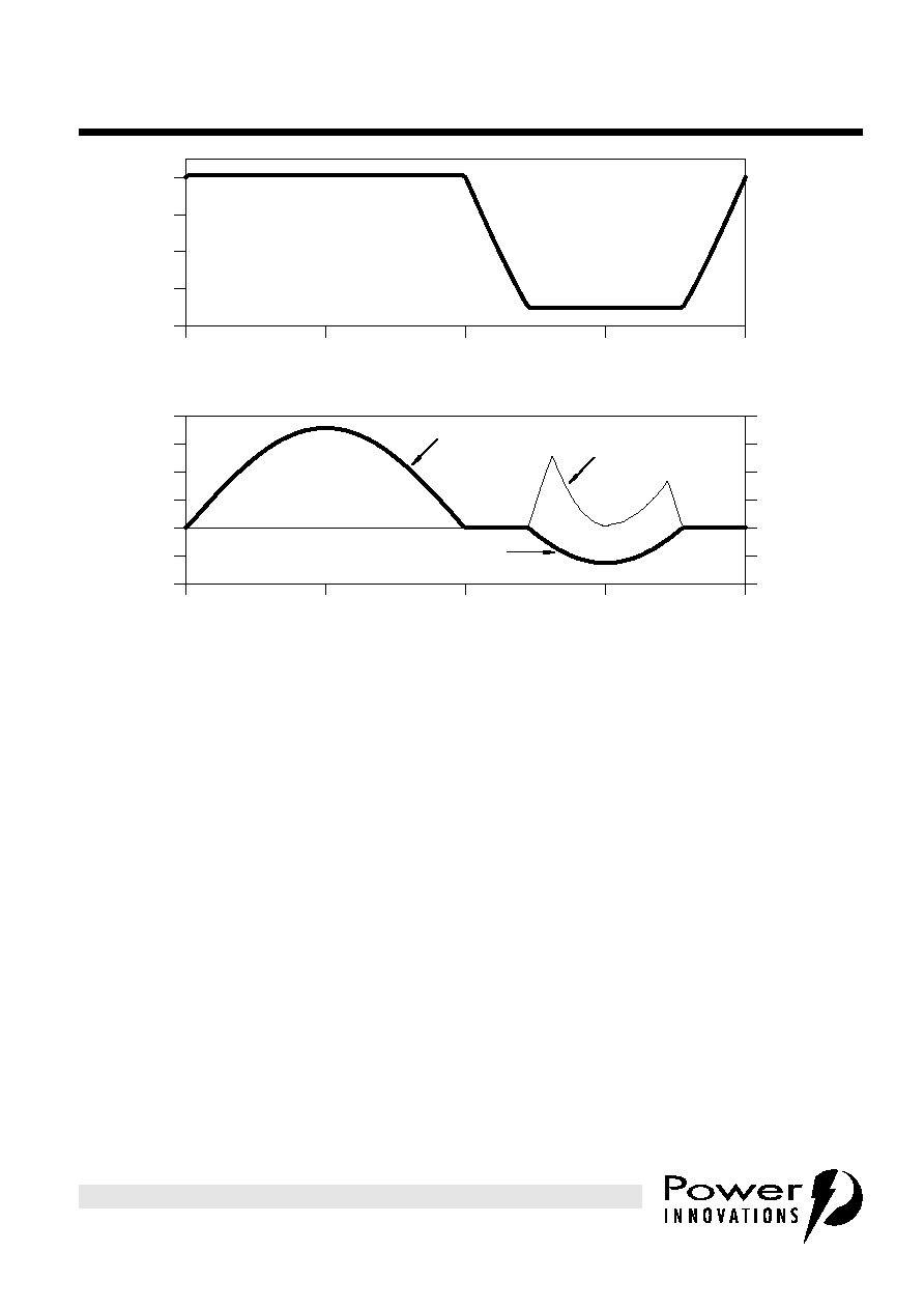
Figure 5 shows the thyristor waveforms under a high impedance power cross condition. Positive half cycles
are clamped to ground by the diodes D1 and D2, producing a peak current of 350 mA. Negative half cycles
are clamped to the -70 V gate supply voltage. The peak cathode current of 120 mA is not enough to cause
thyristor switching. As the thyristor first starts to conduct, the cathode and gate currents are the same. (I
K
=
I
G
). At about 70 mA the thyristor starts to become active and anode current starts to flow. The increasing
anode current progressively reduces the gate current, until the gate current is nearly zero at 15 ms. After that,
Figure 5. PROTECTOR FAST IMPULSE CLAMPING AND SWITCHING WAVEFORMS
V
GG
V
K
Time - µs
0.0
0.5
1.0
1.5
Current - A
-5
-4
-3
-2
-1
0
1
I
K
I
G
Time - µs
0.0
0.5
1.0
1.5
Voltage - V
-80
-60
-40
-20
0
11
DECEMBER 1995 - REVISED SEPTEMBER 1997
R3612
PROGRAMMABLE OVERVOLTAGE PROTECTOR
FOR ERICSSON COMPONENTS 3357/3 DCLIC
P R O D U C T I N F O R M A T I O N
the cathode and anode current decrease, increasing the gate current which peaks for a second time at about
40 mA. The second gate current peak is lower due to the heating caused by the clipping action.
The gate current behaviour is unusual. In the normal common cathode mode operation, once the gate current
reaches its triggering value, I
GT
, the thyristor switches on. In this case the thyristor is being operated in
common gate mode which results in negative feedback. The negative feedback counteracts the thyristors
internal positive feedback (regeneration) preventing switching until the thyristor does not need a gate current
supplement from the gate supply voltage. In common gate mode, thyristor switches at zero gate current and
the gate current peaks earlier as the thyristor starts to become active.
In Figure 5, although the full cycle average gate current is only 6 mA, peaks of 70 mA and 40 mA occur
during the clamping period. This current is a charging current which tries to make the SLIC supply rail even
more negative. If the current drawn by the SLIC is less than the gate current, the SLIC supply rail may
increase to a point where the SLIC suffers an over voltage on its supply rail. In such cases the shunt
avalanche diode, D6, provides the necessary protection by limiting the maximum supply voltage.
IC protectors
In 1986 an IC version was proposed (A 90 V Switching Regulator and Lightning Protection Chip Set, Robert
K. Chen, Thomas H. Lerch, Johnathan S. Radovsky, D. Alan Spires, IEEE Solid-State Circuits Conference,
February 20, 1986, pp 178/9 and pp 340/1). Commercially, this resulted in the AT&T Microelectronics
LB1201AB device and the higher current Texas Instruments Inc. TCM1060 device, Figure 5.
Figure 6. PROTECTOR HIGH IMPEDANCE POWER CROSS CLAMPING WAVEFORMS
Time - ms
0
5
10
15
20
V
K
- Cathode Voltage - V
-80
-60
-40
-20
0
Time - ms
0
5
10
15
20
I
K
- Cathode Current - mA
-200
-100
0
100
200
300
400
I
G
- Gate Current - mA
-50
-25
0
25
50
75
100
I
K
I
K
I
G

R3612
PROGRAMMABLE OVERVOLTAGE PROTECTOR
FOR ERICSSON COMPONENTS 3357/3 DCLIC
12
DECEMBER 1995 - REVISED SEPTEMBER 1997
P R O D U C T I N F O R M A T I O N
To avoid the problems of diode bridge implementation, the thyristor and series gate diode were duplicated
which allowed the bridge series thyristor diodes to be removed. This had the benefit that the protection
voltage was lowered by one diode forward voltage drop. The circuit performance of the IC was similar to the
discrete solution. Due to the integration, when the thyristor was in the on-state or the shunt diode in
conduction, about 10 mA of current was drawn from the gate supply, Figure 5. The direction of this current is
the same as that drawn by the SLIC, so it represented a small additional load on the SLIC supply and resulted
in some additional dissipation in the protector.
buffered gate protectors
The original IC design has been improved in two ways, Figure 5. Firstly, the lateral IC structure has been
changed to a vertical power device structure for increased surge current capability. Second, the series gate
diodes have been changed to transistors. The maximum current injected into the gate supply is then reduced
by the transistors gain factor (H
FE
). In most cases, just the lower peak gate current allows any previously used
SLIC supply rail shunt protection diode to be removed. By designing the protector such that I
GT
< I
GAF
, the net
gate current can be made to be a current drain, rather than a current injection, on the gate supply.
Fast rising surges will initially be clipped to the gate supply via the series combination of thyristor gate-
cathode diode and the transistor base-emitter diode. The overall wave forms will be similar to Figure 5 and the
supply decoupling capacitor, C1, should be dimensioned according to the text that accompanies Figure 5.
Although the SLIC supply is taken to a terminal that is internally connected to transistor bases, the terminal is
designated as the gate terminal, G.
R3612 parameters
The PBA 3357/3 DCLIC is characterised over a 0∞C to 70∞C temperature range. To ensure correct operation,
the R3612 protector is characterised on key paraters over the same temperature range. To ensure service
restoration after an over voltage, the R3612 holding current is 105 mA minimum, which matches the 105 mA
maximum line current of the PBA 3357/3. Typically the PBA3357/3 supply voltage will be -50 V ±6 V, but this
could rise to a maximum rated value of -70 V. To cover these conditions the R3612 is rated at -100 V with
electrical characteristics given at -48 V. The series overcurrent protector characteristic should be coordinated
with the a.c. ratings of the R3612. Overshoot voltages are measured under 0.5/700 µs conditions. This
Figure 7. IC VERSION OF Figure 4
D1
D2
D3
D4
C1
TH1
D6
SLIC
NEGATIVE
SLIC
SUPPLY
TH2
IC
K1
G
K2
A
WIRE A
WIRE B
R1
R2
V
GG

13
DECEMBER 1995 - REVISED SEPTEMBER 1997
R3612
PROGRAMMABLE OVERVOLTAGE PROTECTOR
FOR ERICSSON COMPONENTS 3357/3 DCLIC
P R O D U C T I N F O R M A T I O N
Figure 8. TCM1060 POWER CROSS WAVEFORMS
Figure 9. BUFFERED GATE PROTECTOR
Time - ms
0
5
10
15
20
V
K
- Cathode Voltage - V
-60
-40
-20
0
Time - ms
0
5
10
15
20
I
K
- Cathode Current - mA
-1000
-750
-500
-250
0
250
500
750
1000
I
G
- Gate Current - mA
-75
-50
-25
0
25
50
75
I
K
I
K
I
G
I
G
C1
SLIC
NEGATIVE
SLIC
SUPPLY
D1
D2
T1 T2
TH1
TH2
G
K2
A
WIRE A
WIRE B
R1
R2
V
GG
K1
R3612

R3612
PROGRAMMABLE OVERVOLTAGE PROTECTOR
FOR ERICSSON COMPONENTS 3357/3 DCLIC
14
DECEMBER 1995 - REVISED SEPTEMBER 1997
P R O D U C T I N F O R M A T I O N
particular lightning surge wave shape has the fastest rise time and gives the largest voltage overshoot values.
It is at least 20 times faster than the 10/1000 µs and 10/700 µs surges and so the 0.5/700 µs surge
represents a worse case condition.

15
DECEMBER 1995 - REVISED SEPTEMBER 1997
R3612
PROGRAMMABLE OVERVOLTAGE PROTECTOR
FOR ERICSSON COMPONENTS 3357/3 DCLIC
P R O D U C T I N F O R M A T I O N
P00
plastic dual-in-line package
This dual-in-line package consists of a circuit mounted on a lead frame and encapsulated within a plastic
compound. The compound will withstand soldering temperature with no deformation, and circuit performance
characteristics will remain stable when operated in high humidity conditions The package is intended for
insertion in mounting-hole rows on 7,62 (0.300) centers. Once the leads are compressed and inserted,
sufficient tension is provided to secure the package in the board during soldering. Leads require no
additional cleaning or processing when used in soldered assembly.
MECHANICAL DATA
1
2
3
4
8
7
6
5
10,2 (0.400) MAX
Index
Dot
1,78 (0.070) MAX
4 Places
5,08 (0.200)
MAX
0,51 (0.020)
MIN
2,54 (0.100) T.P.
6 Places
(see Note A)
0,533 (0.021)
0,381 (0.015)
8 Places
3,17 (0.125)
MIN
Seating
Plane
0,36 (0.014)
0,20 (0.008)
8 Places
105∞
90∞
8 Places
6,60 (0.260)
6,10 (0.240)
7,87 (0.310)
7,37 (0.290)
T.P.
C
L
C
L
ALL LINEAR DIMENSIONS ARE IN MILLIMETERS AND PARENTHETICALLY IN INCHES
P008
Designation per JEDEC Std 30:
PDIP-T8
NOTE A: Each pin centerline is located within 0,25 (0.010) of its true longitudinal position
MDXXABA

R3612
PROGRAMMABLE OVERVOLTAGE PROTECTOR
FOR ERICSSON COMPONENTS 3357/3 DCLIC
16
DECEMBER 1995 - REVISED SEPTEMBER 1997
P R O D U C T I N F O R M A T I O N
IMPORTANT NOTICE
Power Innovations Limited (PI) reserves the right to make changes to its products or to discontinue any
semiconductor product or service without notice, and advises its customers to verify, before placing orders, that the
information being relied on is current.
PI warrants performance of its semiconductor products to the specifications applicable at the time of sale in
accordance with PI's standard warranty. Testing and other quality control techniques are utilized to the extent PI
deems necessary to support this warranty. Specific testing of all parameters of each device is not necessarily
performed, except as mandated by government requirements.
PI accepts no liability for applications assistance, customer product design, software performance, or infringement
of patents or services described herein. Nor is any license, either express or implied, granted under any patent
right, copyright, design right, or other intellectual property right of PI covering or relating to any combination,
machine, or process in which such semiconductor products or services might be or are used.
PI SEMICONDUCTOR PRODUCTS ARE NOT DESIGNED, INTENDED, AUTHORIZED, OR WARRANTED TO BE
SUITABLE FOR USE IN LIFE-SUPPORT APPLICATIONS, DEVICES OR SYSTEMS.
Copyright © 1997, Power Innovations Limited