 | –≠–ª–µ–∫—Ç—Ä–æ–Ω–Ω—ã–π –∫–æ–º–ø–æ–Ω–µ–Ω—Ç: TCM1030P | –°–∫–∞—á–∞—Ç—å:  PDF PDF  ZIP ZIP |
TISP61060D, TISP61060P
DUAL FORWARD-CONDUCTING P-GATE THYRISTORS
PROGRAMMABLE OVERVOLTAGE PROTECTORS
P R O D U C T I N F O R M A T I O N
1
SEPTEMBER 1995 - REVISED SEPTEMBER 1997
Copyright © 1997, Power Innovations Limited, UK
Information is current as of publication date. Products conform to specifications in accordance
with the terms of Power Innovations standard warranty. Production processing does not
necessarily include testing of all parameters.
PROGRAMMABLE SLIC OVERVOLTAGE PROTECTION
q
Dual Voltage-Programmable Protectors
- Third Generation Design using Vertical
Power Technology
- Wide -5 V to -85 V Programming Range
- High 150 mA min. Holding Current
q
Reduced V
BAT
Supply Current
- Triggering Current is Typically 50x Lower
- Negative Value Power Induction Current
Removes Need for Extra Protection Diode
q
Rated for LSSGR & FCC Surges
q
Surface Mount and Through-Hole Options
- TISP61060P for Plastic DIP
- TISP61060D for Small-Outline
- TISP61060DR for Taped and Reeled
Small-Outline
q
Functional Replacements for
description
The TISP61060 is a dual forward-conducting
buffered p-gate overvoltage protector. It is
designed to protect monolithic SLICs (Subscriber
Line Interface Circuits), against overvoltages on
the telephone line caused by lightning, a.c.
power contact and induction. The TISP61060
limits voltages that exceed the SLIC supply rail
voltage.
STANDARD
WAVE SHAPE
I
TSP
A
LSSGR
10/1000 µs
30
FCC Part 68
10/160 µs
45
LSSGR
2/10 µs
50
PART NUMBERS
FUNCTIONAL
REPLACEMENT
TCM1030P, TCM1060P, LB1201AB
TISP61060P
TCM1030D, TCM1060D, LB1201AS
TISP61060D
TCM1030DR, TCM1060DR
TISP61060DR
The SLIC line driver section is typically powered from 0 V (ground) and a negative voltage in the region of
-10 V to -70 V. The protector gate is connected to this negative supply. This references the protection
(clipping) voltage to the negative supply voltage. As the protection voltage will track the negative supply
voltage, the overvoltage stress on the SLIC is minimised. (see Applications Information).
Positive overvoltages are clipped to ground by diode forward conduction. Negative overvoltages are initially
clipped close to the SLIC negative supply rail value. If sufficient current is available from the overvoltage, then
the protector will crowbar into a low voltage on-state condition. As the current subsides the high holding
current of the crowbar prevents d.c. latchup.
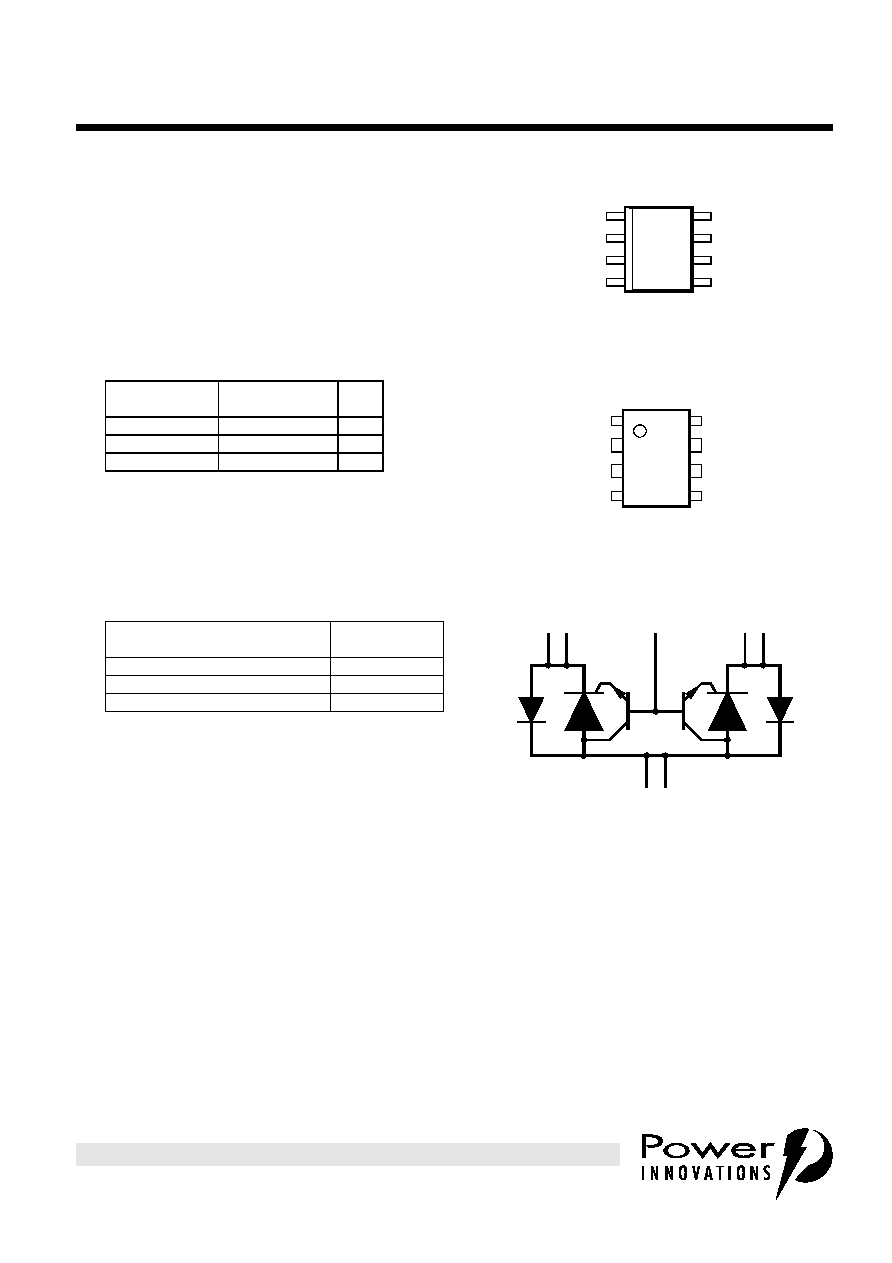
device symbol
Terminals K1, K2 and A correspond to the alternative
line designators of T, R and G or A, B and C. The
negative protection voltage is controlled by the voltage,
V
GG,
applied to the G terminal.
SD6XAE
A
K1
G
K2
MD6XAO
'61060D PACKAGE
(TOP VIEW)
NC - No internal connection
Terminal typical application names shown in
parenthesis
1
2
3
4
5
6
7
8
K1
A
A
K2
G
K1
K2
NC
(Tip)
(Ground)
(Ground)
(Ring)
(V
S
)
(Tip)
(Ring)
MD6XAP
'61060P PACKAGE
(TOP VIEW)
NC - No internal connection
Terminal typical application names shown in
parenthesis
1
2
3
4
5
6
7
8
K2
G
K1
NC
K1
A
A
K2
(Tip)
(Ground)
(Ground)
(Ring)
(V
S
)
(Tip)
(Ring)

TISP61060D, TISP61060P
DUAL FORWARD-CONDUCTING P-GATE THYRISTORS
PROGRAMMABLE OVERVOLTAGE PROTECTORS
2
SEPTEMBER 1995 - REVISED SEPTEMBER 1997
P R O D U C T I N F O R M A T I O N
These monolithic protection devices are fabricated in ion-implanted planar vertical power structures for high
reliability and in normal system operation they are virtually transparent. The buffered gate design reduces the
loading on the SLIC supply during overvoltages caused by power cross and induction.
NOTES: 1. Initially the protector must be in thermal equilibrium with -40∞C
T
J
85∞C. The surge may be repeated after the device returns to
its initial conditions.
2. The rated current values may be applied either to the Ring to Ground or to the Tip to Ground terminal pairs. Additionally, both
terminal pairs may have their rated current values applied simultaneously (in this case the Ground terminal current will be twice the
rated current value of an individual terminal pair). Above 85∞C, derate linearly to zero at 150∞C lead temperature.
absolute maximum ratings
RATING
SYMBOL
VALUE
UNIT
Repetitive peak off-state voltage, I
G
= 0, -40∞C
T
J
85∞C
V
DRM
-100
V
Repetitive peak gate-cathode voltage, V
KA
= 0, -40∞C
T
J
85∞C
V
GKRM
-85
V
Non-repetitive peak on-state pulse current (see Notes 1 and 2)
I
TSP
A
10/1000 µs
30
10/160 µs
45
2/10 µs
50
Non-repetitive peak on-state current (see Notes 1 and 2)
I
TSM
Arms
60 Hz sine-wave, 25 ms
6
60 Hz sine-wave, 2 s
1
Continuous on-state current (see Note 2)
I
TM
0.3
A
Continuous forward current (see Note 2)
I
FM
0.3
A
Operating free-air temperature range
T
A
-40 to +85
∞C
Storage temperature range
T
stg
-40 to +150
∞C
Lead temperature 1,6 mm (1/16 inch) from case for 10 s
T
L
260
∞C
recommended operating conditions
MIN
TYP
MAX
UNIT
C
G
Gate decoupling capacitor
100
nF
electrical characteristics, -40∞C
T
J
85∞C (unless otherwise noted)
PARAMETER
TEST CONDITIONS
MIN
TYP
MAX
UNIT
I
D
Off-state current
V
D
= -85 V, V
GK
= 0 V
T
J
= 25∞C
5
µA
T
J
= 85∞C
50
µA
V
(BO)
Breakover voltage
dv/dt = -250 V/ms, Source Resistance = 300
, V
GG
= -50 V
dv/dt = -250 V/ms, Source Resistance = 300
, V
GG
= -65 V
I
T
= 12.5 A, 10/1000 µs, Source Resistance = 80
, V
GG
= -50 V
-53
-68
-55
V
I
S
Switching current
dv/dt = -250 V/ms, Source Resistance = 300
, V
GG
= -50 V
-100
mA
V
T
On-state voltage
I
T
= 1 A
I
T
= 10 A
I
T
= 16 A
I
T
= 30 A
3
4
5
7
V
V
F
Forward voltage
I
F
= 1 A
I
F
= 10 A
I
F
= 16 A
I
F
= 30 A
2
4
5
5
V
I
H
Holding current
I
T
= -1 A, di/dt = +1A/ms, V
GG
= -50 V
-150
mA
3
SEPTEMBER 1995 - REVISED SEPTEMBER 1997
TISP61060D, TISP61060P
DUAL FORWARD-CONDUCTING P-GATE THYRISTORS
PROGRAMMABLE OVERVOLTAGE PROTECTORS
P R O D U C T I N F O R M A T I O N
I
GAS
Gate reverse current
V
GG
= -85 V, K and A terminals connected
T
J
= 25∞C
5
µA
T
J
= 85∞C
50
µA
I
GT
Gate trigger current
I
T
= -1 A, t
p(g)
20 µs, V
GG
= -50 V
15
mA
dv/dt
Critical rate of rise of
off-state voltage
V
GG
= -50 V, (see Note 3)
-1000
V/µs
C
O
Anode-cathode off-
state capacitance
f = 1 MHz, V
d
= 0.1 V, I
G
= 0, (see Note 4)
V
D
= 0 V
85
pF
V
D
= -50 V
10
pF
NOTES: 3. Linear rate of rise, maximum voltage limited to 80% V
GG
.
4. These capacitance measurements employ a three terminal capacitance bridge incorporating a guard circuit. The unmeasured
device terminals are a.c. connected to the guard terminal of the bridge.
thermal characteristics
PARAMETER
TEST CONDITIONS
MIN
TYP
MAX
UNIT
R
JA
Junction to free air thermal resistance
P
tot
= 0.8 W, T
A
= 25∞C
5 cm
2
, FR4 PCB
D Package
170
∞C/W
P Package
125
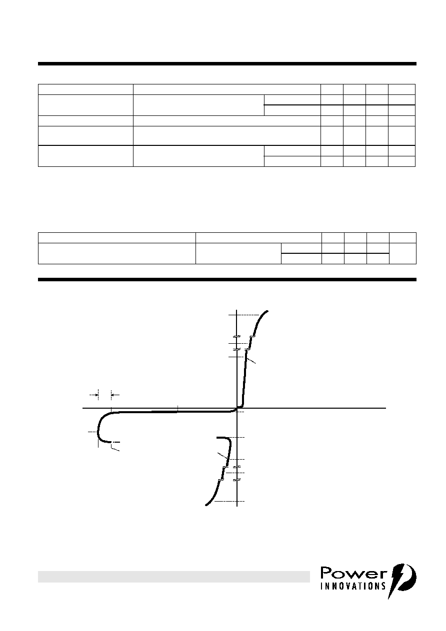
PARAMETER MEASUREMENT INFORMATION
Figure 1. VOLTAGE-CURRENT CHARACTERISTIC
electrical characteristics, -40∞C
T
J
85∞C (unless otherwise noted) (continued)
PARAMETER
TEST CONDITIONS
MIN
TYP
MAX
UNIT
-v
I
S
V
S
V
GG
V
D
I
H
I
T
V
T
I
TSM
I
TSP
V
(BO)
I
(BO)
I
D
Quadrant I
Forward
Conduction
Characteristic
+v
+i
I
F
V
F
I
FSM
(= |I
TSM
|)
I
FSP
(= |I
TSP
|)
-i
Quadrant III
Switching
Characteristic
PM6XAAA
V
GK(BO)

TISP61060D, TISP61060P
DUAL FORWARD-CONDUCTING P-GATE THYRISTORS
PROGRAMMABLE OVERVOLTAGE PROTECTORS
4
SEPTEMBER 1995 - REVISED SEPTEMBER 1997
P R O D U C T I N F O R M A T I O N
DEVICE PARAMETERS
general
Thyristor based overvoltage protectors, for telecommunications equipment, became popular in the late
1970s. These were fixed voltage breakover triggered devices, likened to solid state gas discharge tubes. As
these were new forms of thyristor, the existing thyristor terminology did not cover their special characteristics.
This resulted in the invention of new terms based on the application usage and device characteristic. Initially,
there was a wide diversity of terms to describe the same thing, but today the number of terms have reduced
and stabilised.
Programmable, (gated), overvoltage protectors are relatively new and require additional parameters to
specify their operation. Similarly to the fixed voltage protectors, the introduction of these devices has resulted
in a wide diversity of terms to describe the same thing. To help promote an understanding of the terms and
their alternatives, this section has a list of alternative terms and the parameter definitions used for this data
sheet. In general, the Texas Instruments approach is to use terms related to the device internal structure,
rather than its application usage as a single device may have many applications each using a different
terminology for circuit connection.
alternative symbol cross-reference guide
This guide is intended to help the translation of alternative symbols to those used in this data sheet. As in
some cases the alternative symbols have no substance in international standards and are not fully defined by
the originators, users must confirm symbol equivalence. No liability will be assumed from the use of this
guide.
CROSS-REFERENCE FOR TISP61060 AND TCM1030/60
TISP61060 PARAMETER
DATA SHEET
SYMBOL
ALTERNATIVE
SYMBOL
ALTERNATIVE PARAMETER
RATINGS & CHARACTERISTICS
TCM1060, TCM1030
Non-repetitive peak on-state pulse current
I
TSP
-
Non-repetitive peak surge current
Non-repetitive peak on-state current
I
TSM
-
Non-repetitive peak surge current,10 ms
Non-repetitive peak on-state current
I
TSM
-
Continuous 60-Hz sinewave, 2 s
Forward voltage
V
F
V
CF
Forward clamping voltage
Forward current
I
F
I
FM
Peak forward current
On-state voltage
V
T
V
C
Reverse clamping voltage
On-state current
I
T
I
TM
Peak reverse current
Switching current
I
S
I
trip
Trip current
Breakover voltage
V
(BO)
V
trip
Trip voltage
Gate reverse current (with A and K terminals connected)
I
GAS
I
D
Stand-by current, TIP & RING at GND
Off-state current
I
D
I
D
Stand-by current, TIP & RING at V
S
Off-state voltage
V
D
V
S
Supply voltage
Gate-cathode breakover voltage
V
GK(BO)
V
OS
Transient overshoot voltage
Gate voltage, (V
GG
is gate supply voltage referenced
to the A terminal)
V
G
V
S
Supply voltage
Off-state capacitance
C
O
C
off
Off-state capacitance
TERMINALS
TCM1060, TCM1030
Cathode 1
K1
Tip
Tip
Cathode 2
K2
Ring
Ring
Anode
A
GND
Ground
Gate
G
V
S
Supply voltage
5
SEPTEMBER 1995 - REVISED SEPTEMBER 1997
TISP61060D, TISP61060P
DUAL FORWARD-CONDUCTING P-GATE THYRISTORS
PROGRAMMABLE OVERVOLTAGE PROTECTORS
P R O D U C T I N F O R M A T I O N
APPLICATIONS INFORMATION
electrical characteristics
The electrical characteristics of a thyristor overvoltage protector are strongly dependent on junction
temperature, T
J
. Hence a characteristic value will depend on the junction temperature at the instant of
measurement. The values given in this data sheet were measured on commercial testers, which generally
minimise the temperature rise caused by testing.
gated protector evolution and characteristics
This section covers three topics. Firstly, it is explained why gated protectors are needed. Second, the
performance of the original IC (integrated circuit) based version is described. Third, the performance
improvements given by the TISP61060 are detailed.
purpose of gated protectors
Fixed voltage thyristor overvoltage protectors have been used since the early 1980s to protect monolithic
SLICs (Subscriber Line Interface Circuits) against overvoltages on the telephone line caused by lightning, a.c.
power contact and induction. As the SLIC was usually powered from a fixed voltage negative supply rail, the
limiting voltage of the protector could also be a fixed value. The TISP1072F3 is a typical example of a fixed
voltage SLIC protector.
SLICs have become more sophisticated. To minimise power consumption, some designs automatically adjust
the supply voltage, V
BAT
, to a value that is just sufficient to drive the required line current. For short lines the
supply voltage would be set low, but for long lines, a higher supply voltage would be generated to drive
sufficient line current. The optimum protection for this type of SLIC would be given by a protection voltage
which tracks the SLIC supply voltage. This can be achieved by connecting the protection thyristor gate to the
SLIC supply, Figure 2. This gated (programmable) protection arrangement minimises the voltage stress on
the SLIC, no matter what value of supply voltage.
CROSS-REFERENCE FOR TISP61060 AND LB1201AB
TISP61060 PARAMETER
DATA SHEET
SYMBOL
ALTERNATIVE
SYMBOL
ALTERNATIVE PARAMETER
RATINGS & CHARACTERISTICS
LB1201AB
Non-repetitive peak on-state pulse current
I
TSP
I
P
Pulse current
Non-repetitive peak on-state current
I
TSM
I
P
RMS pulse current, 60 Hz
On-state voltage
V
T
V
ON
On-state voltage
Switching current
I
S
I
t
Trip current
Breakover voltage
V
(BO)
V
T
Trip voltage
Maximum continuous on-state current
I
TM
I
C
On-state current
Maximum continuous forward current
I
FM
I
C
On-state current
Gate voltage, (V
GG
is gate supply voltage referenced
to the A terminal)
V
G
V
S
Supply voltage
Off-state capacitance
C
O
C
OFF
Off-state capacitance
TERMINALS
LB1201AB
Cathode 1
K1
Tip
Tip
Cathode 2
K2
Ring
Ring
Anode
A
GND
Ground
Gate
G
V
S
Supply voltage