Specifications are subject to change without notice.
186
JUNE 2001
TISP4xxxH3/M3BJ Series for LCAS Protection
TISP4125H3BJ/TISP4219H3BJ,
TISP4125M3BJ/TISP4219M3BJ
LCAS RING AND TIP PROTECTION PAIRS
BIDIRECTIONAL THYRISTOR OVERVOLTAGE PROTECTORS
Description
Customized Voltage for LCAS Protection
Battery-Backed Ringing ............................................. 87 V rms
Ground-Backed Ringing ........................................... 101 V rms
Low Differential Capacitance ................................. 39 pF max.
.................................................... UL Recognized Components
Rated for International Surge Wave Shapes
These protector pairs have been formulated to limit the peak voltages on the line terminals of the `7581/2/3 LCAS (Line Card Access Switches)
type devices. An LCAS may also be referred to as a Solid State Relay, SSR, i.e. a replacement of the conventional electro-mechanical relay.
Overvoltages are normally caused by a.c. power system or lightning flash disturbances which are induced or conducted on to the telephone
line. These overvoltages are initially clipped by protector breakdown clamping until the voltage rises to the breakover level, which causes the
device to crowbar into a low-voltage on state. This low-voltage on state causes the current resulting from the overvoltage to be safely diverted
through the device. For negative surges, the high crowbar holding current prevents d.c. latchup with the SLIC current, as the surge current
subsides.
Each protector consists of a symmetrical voltage-triggered bidirectional thyristor. They are guaranteed to voltage limit and withstand the listed
international lightning surges in both polarities.
How to Order
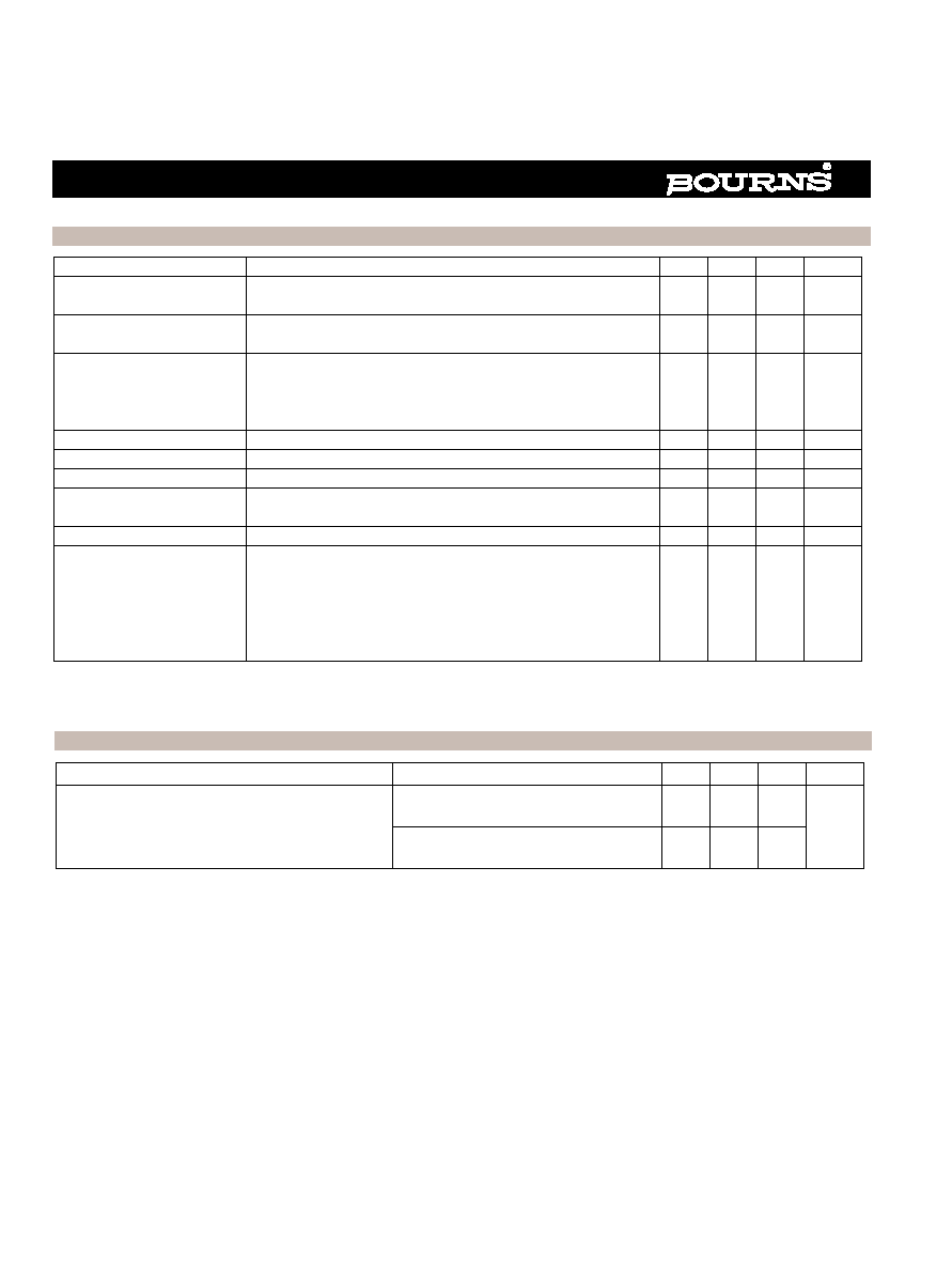
Device Symbol
SMBJ Package (Top View)
Device
V
DRM
V
V
(BO)
V
LCAS
TERMINAL
`4125
100
125
TIP
`4219
180
219
RING
Wave Shape
Standard
I
TSP
A
H3
SERIES
M3
SERIES
2/10
µs
GR-1089-CORE
500
300
8/20
µs
IEC 61000-4-5
300
220
10/160
µs
FCC Part 68
250
120
10/700
µs
ITU-T K.20/21/45
200
100
10/560
µs
FCC Part 68
160
75
10/1000
µs
GR-1089-CORE
100
50
1
2
T( A)
R(B)
MDXXBGE
T
R
SD4XAA
Terminals T and R correspond to the
alternative line designators of A and B
Device
Package
Carrier
Order As
TISP4125H3B J
BJ (J-Bend DO-214AA/SMB) Embossed Tape Reeled
TISP4125H3B JR
TISP4219H3B J
TISP4219H3B JR
TISP4125M3BJ
TISP4125M3BJR
TISP4219M3BJ
TISP4219M3BJR

Specifications are subject to change without notice.
187
JUNE 2001
Absolute Maximum Ratings, TA = 25 ∞C (Unless Otherwise Noted)
TISP4xxxH3/M3BJ Series for LCAS Protection
Recommended Operating Conditions
Component
Condition
Min
Typ
Max
Unit
R
S
Series current limiting
resistor
GR-1089-CORE first-level surge survival
0
GR-1089-CORE first-level and second-level surge survival
0
K.20, K.21 and K.45 coordination pass with a 400 V primary
protector
6
V
RING
AC ringing voltage
Figure 12, V
BAT
= -48 V
±2.5 V,
R1= R2 = 300
, 0
∞C < T
A
< +85
∞C
Battery-backed
87
V rms
V rms
Ground-backed
101
TISP4125H3BJ & TISP4219H3BJ
Rating
Symbol
Value
Unit
Repetitive peak off-state voltage, (see Note 1)
`4125
`4219
V
DRM
±100
±180
V
Non-repetitive peak on-state pulse current (see Notes 2 and 3)
I
TSP
A
2/10
µs (GR-1089-CORE, 2/10 µs voltage wave shape)
500
8/20
µs (IEC 61000-4-5, 1.2/50 µs voltage, 8/20 current combination wave generator)
300
10/160
µs (FCC Part 68, 10/160 µs voltage wave shape)
250
5/200
µs (VDE 0433, 10/700 µs voltage wave shape)
220
0.2/310
µs (I3124, 0.5/700 µs voltage wave shape)
200
5/310
µs (ITU-T K.20/21, 10/700 µs voltage wave shape)
200
5/310
µs (FTZ R12, 10/700 µs voltage wave shape)
200
10/560
µs (FCC Part 68, 10/560 µs voltage wave shape)
160
10/1000
µs (GR-1089-CORE, 10/1000 µs voltage wave shape)
100
Non-repetitive peak on-state current (see Notes 2, 3 and 4)
I
TSM
55
60
2.1
A
20 ms (50 Hz) full sine wave
16.7 ms (60 Hz) full sine wave
1000 s 50 Hz/60 Hz a.c.
Initial rate of rise of on-state current,
Exponential current ramp, Maximum ramp value < 200 A
di
T
/dt
400
A/
µs
Junction temperature
T
J
-40 to +150
∞C
Storage temperature range
T
stg
-65 to +150
∞C
NOTES: 1. See Applications Information for voltage values at lower temperatures.
2. Initially, the TISP4xxxH3BJ must be in thermal equilibrium with T
J
= 25
∞C.
3. The surge may be repeated after the TISP4xxxH3BJ returns to its initial conditions.
4. EIA/JESD51-2 environment and EIA/JESD51-3 PCB with standard footprint dimensions connected with 5 A rated printed wiring
track widths. See Figure 10 for the current ratings at other durations. Derate current values at -0.61 %/
∞C for ambient
temperatures above 25
∞C.

Specifications are subject to change without notice.
188
JUNE 2001
TISP4xxxH3/M3BJ Series for LCAS Protection
Electrical Characteristics, TISP4xxxH3, TA = 25 ∞C (Unless Otherwise Noted)
Thermal Characteristics
Parameter
Test Conditions
Min
Typ
Max
Unit
I
DRM
Repetitive peak off-
state current
V
D
= V
DRM
T
A
= 25
∞C
T
A
= 85
∞C
±5
±10
µA
V
(BO)
Breakover voltage
dv/dt =
±250 V/ms, R
SOURCE
= 300
`4125
`4219
±125
±219
V
V
(BO)
Impulse breakover
voltage
dv/dt
±1000 V/µs, Linear voltage ramp,
Maximum ramp value =
±500 V
di/dt =
±20 A/µs, Linear current ramp,
Maximum ramp value =
±10 A
`4125
`4219
±134
±229
V
I
(BO)
Breakover current
dv/dt =
±250 V/ms, R
SOURCE
= 300
±0.15
±0.6
A
V
T
On-state voltage
I
T
=
±5 A, t
W
= 100
µs
±3
V
I
H
Holding current
I
T
=
±5 A, di/dt = +/-30 mA/ms
±0.15
±0.6
A
dv/dt
Critical rate of rise of
off-state voltage
Linear voltage ramp, Maximum ramp value < 0.85V
DRM
±5
kV/
µs
I
D
Off-state current
V
D
=
±50 V
T
A
= 85
∞C
±10
µA
C
off
Off-state capacitance
f = 1 MHz,
V
d
= 1 V rms, V
D
= 0,
f = 1 MHz,
V
d
= 1 V rms, V
D
= -1 V
f = 1 MHz,
V
d
= 1 V rms, V
D
= -2 V
f = 1 MHz,
V
d
= 1 V rms, V
D
= -50 V
f = 1 MHz,
V
d
= 1 V rms, V
D
= -100 V
(see Note 5)
80
71
65
30
23
90
79
74
35
28
pF
NOTE 5: To avoid possible voltage clipping, the `4125 is tested with V
D
= -98 V.
Parameter
Test Conditions
Min
Typ
Max
Unit
R
JA
Junction to free air thermal resistance
EIA/JESD51-3 PCB, I
T
= I
TSM(1000)
,
T
A
= 25
∞C, (see Note 6)
113
∞C/W
265 mm x 210 mm populated line card,
4-layer PCB, I
T
= I
TSM(1000)
, T
A
= 25
∞C
50
NOTE
6: EIA/JESD51-2 environment and the PCB has standard footprint dimensions connected with 5 A rated printed wiring track widths.

Specifications are subject to change without notice.
189
JUNE 2001
TISP4xxxH3/M3BJ Series for LCAS Protection
Absolute Maximum Ratings, TA = 25 ∞C (Unless Otherwise Noted)
Rating
Symbol
Value
Unit
Repetitive peak off-state voltage, (see Note 7)
`4125
`4219
V
DRM
±100
±180
V
Non-repetitive peak on-state pulse current (see Notes 8 and 9)
I
TSP
A
2/10
µs (GR-1089-CORE, 2/10 µs voltage wave shape)
300
8/20
µs (IEC 61000-4-5, 1.2/50 µs voltage, 8/20 current combination wave generator)
220
10/160
µs (FCC Part 68, 10/160 µs voltage wave shape)
120
5/200
µs (VDE 0433, 10/700 µs voltage wave shape)
110
0.2/310
µs (I3124, 0.5/700 µs voltage wave shape)
100
5/310
µs (ITU-T K.20/21, 10/700 µs voltage wave shape)
100
5/310
µs (FTZ R12, 10/700 µs voltage wave shape)
100
10/560
µs (FCC Part 68, 10/560 µs voltage wave shape)
75
10/1000
µs (GR-1089-CORE, 10/1000 µs voltage wave shape)
50
Non-repetitive peak on-state current (see Notes 8, 9 and 10)
I
TSM
30
32
2.1
A
20 ms (50 Hz) full sine wave
16.7 ms (60 Hz) full sine wave
1000 s 50 Hz/60 Hz a.c.
Initial rate of rise of on-state current,
Exponential current ramp, Maximum ramp value < 200 A
di
T
/dt
300
A/
µs
Junction temperature
T
J
-40 to +150
∞C
Storage temperature range
T
stg
-65 to +150
∞C
NOTES: 7. See Applications Information for voltage values at lower temperatures.
8. Initially, the TISP4xxxM3BJ must be in thermal equilibrium with T
J
= 25
∞C.
9. The surge may be repeated after the TISP4xxxM3BJ returns to its initial conditions.
10. EIA/JESD51-2 environment and EIA/JESD51-3 PCB with standard footprint dimensions connected with 5 A rated printed wiring
track widths. See Figure 11 for the current ratings at other durations. Derate current values at -0.61 %/
∞C for ambient
temperatures above 25
∞C.
Recommended Operating Conditions
Component
Condition
Min
Typ
Max
Unit
R
S
Series current limiting
resistor
GR-1089-CORE first-level surge survival
10
GR-1089-CORE first-level and second-level surge survival
12
K.20, K.21 and K.45 coordination pass with a 400 V primary
protector
6
V
RING
AC ringing voltage
Figure 12, V
BAT
= -48 V
±2.5 V,
R1= R2 = 300
, 0
∞C < T
A
< +85
∞C
Battery-backed
87
V rms
V rms
Ground-backed
101
TISP4125M3BJ & TISP4219M3BJ
Specifications are subject to change without notice.
190
JUNE 2001
TISP4xxxH3/M3BJ Series for LCAS Protection
Electrical Characteristics, TISP4xxxM3, TA = 25 ∞C (Unless Otherwise Noted)
Parameter
Test Conditions
Min
Typ
Max
Unit
I
DRM
Repetitive peak off-
state current
V
D
= V
DRM
T
A
= 25
∞C
T
A
= 85
∞C
±5
±10
µA
V
(BO)
Breakover voltage
dv/dt =
±250 V/ms, R
SOURCE
= 300
`4125
`4219
±125
±219
V
V
(BO)
Impulse breakover
voltage
dv/dt
±1000 V/µs, Linear voltage ramp,
Maximum ramp value =
±500 V
di/dt =
±20 A/µs, Linear current ramp,
Maximum ramp value =
±10 A
`4125
`4219
±132
±226
V
I
(BO)
Breakover current
dv/dt =
±250 V/ms, R
SOURCE
= 300
±0.15
±0.6
A
V
T
On-state voltage
I
T
=
±5 A, t
W
= 100
µs
±3
V
I
H
Holding current
I
T
=
±5 A, di/dt = +/-30 mA/ms
±0.15
±0.6
A
dv/dt
Critical rate of rise of
off-state voltage
Linear voltage ramp, Maximum ramp value < 0.85V
DRM
±5
kV/
µs
I
D
Off-state current
V
D
=
±50 V
T
A
= 85
∞C
±10
µA
C
off
Off-state capacitance
f = 1 MHz,
V
d
= 1 V rms, V
D
= 0,
f = 1 MHz,
V
d
= 1 V rms, V
D
= -1 V
f = 1 MHz,
V
d
= 1 V rms, V
D
= -2 V
f = 1 MHz,
V
d
= 1 V rms, V
D
= -50 V
f = 1 MHz,
V
d
= 1 V rms, V
D
= -100 V
(see Note 11)
62
56
52
26
21
74
67
62
31
25
pF
NOTE 11: To avoid possible voltage clipping, the `4125 is tested with V
D
= -98 V.
Thermal Characteristics
Parameter
Test Conditions
Min
Typ
Max
Unit
R
JA
Junction to free air thermal resistance
EIA/JESD51-3 PCB, I
T
= I
TSM(1000)
,
T
A
= 25
∞C, (see Note 12)
115
∞C/W
265 mm x 210 mm populated line card,
4-layer PCB, I
T
= I
TSM(1000)
, T
A
= 25
∞C
52
NOTE 12: EIA/JESD51-2 environment and the PCB has standard footprint dimensions connected with 5 A rated printed wiring track widths.

Specifications are subject to change without notice.
191
JUNE 2001
TISP4xxxH3/M3BJ Series for LCAS Protection
Parameter Measurement Information
Figure 1. Voltage-Current Characteristic for T and R Terminals
All Measurements are Referenced to the R Terminal
-v
V
DRM
I
DRM
V
D
I
H
I
T
V
T
I
TSM
I
TSP
V
(BO)
I
(BO)
I
D
Quadrant I
I
Switching
Characteristic
+v
+i
V
(BO)
I
(BO)
V
D
I
D
I
H
I
T
V
T
I
TSM
I
TSP
-i
Quadrant III
Switching
Characteristic
PMXXAAB
V
DRM
I
DRM

Specifications are subject to change without notice.
192
JUNE 2001
TISP4xxxH3/M3BJ Series for LCAS Protection
TISP4xxxH3BJ Typical Characteristics
Figure 2.
OFF-STATE CURRENT
vs
JUNCTION TEMPERATURE
T
J
- Junction Temperature -
∞C
-25
0
25
50
75
100
125
150
|I
D
| -
Of
f-State Curr
ent -
µ
A
0∑001
0∑01
0∑1
1
10
100
TCHAG
V
D
=
±50 V
Figure 4.
ON-STATE CURRENT
vs
ON-STATE VOLTAGE
V
T
- On-State Voltage - V
0.7
1.5
2
3
4
5
7
1
10
I
T
-
On-State Curr
e
nt - A
1.5
2
3
4
5
7
15
20
30
40
50
70
150
200
1
10
100
T
A
= 25
∞C
t
W
= 100
µs
TC4HACC
Figure 5.
NORMALIZED HOLDING CURRENT
vs
JUNCTION TEMPERATURE
T
J
- Junction Temperature -
∞C
-25
0
25
50
75
100
125
150
Normalized Holding Curr
ent
0.4
0.5
0.6
0.7
0.8
0.9
1.5
2.0
1.0
TC4HAD
Figure 3.
NORMALIZED BREAKOVER VOLTAGE
vs
JUNCTION TEMPERATURE
T
J
- Junct ion Temperature -
∞C
-25
0
25
50
75
100
125
150
Normalized Br
eakover V
oltage
0.95
1.00
1.05
1.10
TC4HAF

Specifications are subject to change without notice.
193
JUNE 2001
TISP4xxxH3/M3BJ Series for LCAS Protection
TISP4xxxM3BJ Typical Characteristics
OFF-STATE CURRENT
vs
JUNCTION TEMPERATURE
T
J
- Junction Temperature -
∞C
Of
f-State Curr
ent -
µ
A
Figure 6.
-25
0
25
50
75
100
125
150
|I
D
| -
0∑001
0∑01
0∑1
1
10
100
TCMAG
V
D
=
±50 V
NORMALIZED BREAKOVER VOLTAGE
vs
JUNCTION TEMPERATURE
Figure 7.
T
J
- Junct ion Temperature -
∞C
Normalized Br
eakover V
oltage
-25
0
25
50
75
100
125
150
0.95
1.00
1.05
1.10
TC4MAF
ON-STATE CURRENT
vs
ON-STATE VOLTAGE
On-State Curr
ent - A
Figure 8.
V
T
- On-State Voltage - V
0.7
1.5
2
3
4
5
7
1
10
I
T
-
1.5
2
3
4
5
7
15
20
30
40
50
70
1
10
100
T
A
= 25
∞C
t
W
= 100
µs
TC4MACB
NORMALIZED HOLDING CURRENT
vs
JUNCTION TEMPERATURE
T
J
- Junction Temperature -
∞C
Normalized Holding Curr
ent
Figure 9.
-25
0
25
50
75
100
125
150
0.4
0.5
0.6
0.7
0.8
0.9
1.5
2.0
1.0
TC4MAD

Specifications are subject to change without notice.
194
JUNE 2001
TISP4xxxH3/M3BJ Series for LCAS Protection
Rating Information
TISP4xxxH3BJ
Figure 10.
NON-REPETITIVE PEAK ON-STATE CURRENT
vs
CURRENT DURATION
t - Current Duration - s
0∑1
1
10
100
1000
I
TS
M(t)
-
Non-Repetitive Peak On-State Curr
ent - A
1.5
2
3
4
5
6
7
8
9
15
20
30
10
TI4HAC
V
GEN
= 600 Vrms, 50/60 Hz
R
GEN
= 1.4*V
GEN
/I
TSM(t)
EIA/JESD51-2 ENVIRONMENT
EIA/JESD51-3 PCB
T
A
= 25
∞C
TISP4xxxM3BJ
Figure 11.
NON-REPETITIVE PEAK ON-STATE CURRENT
vs
CURRENT DURATION
t - Current Duration - s
Non-Repetitive Peak On-State Curr
ent - A
0∑1
1
10
100
1000
I
TS
M(t)
-
1.5
2
3
4
5
6
7
8
9
15
20
30
10
TI4MAC
V
GEN
= 600 Vrms, 50/60 Hz
R
GEN
= 1.4*V
GEN
/I
TSM(t)
EIA/JESD51-2 ENVIRONMENT
EIA/JESD51-3 PCB
T
A
= 25
∞C
Specifications are subject to change without notice.
195
JUNE 2001
TISP4xxxH3/M3BJ Series for LCAS Protection
APPLICATIONS INFORMATION
Introduction
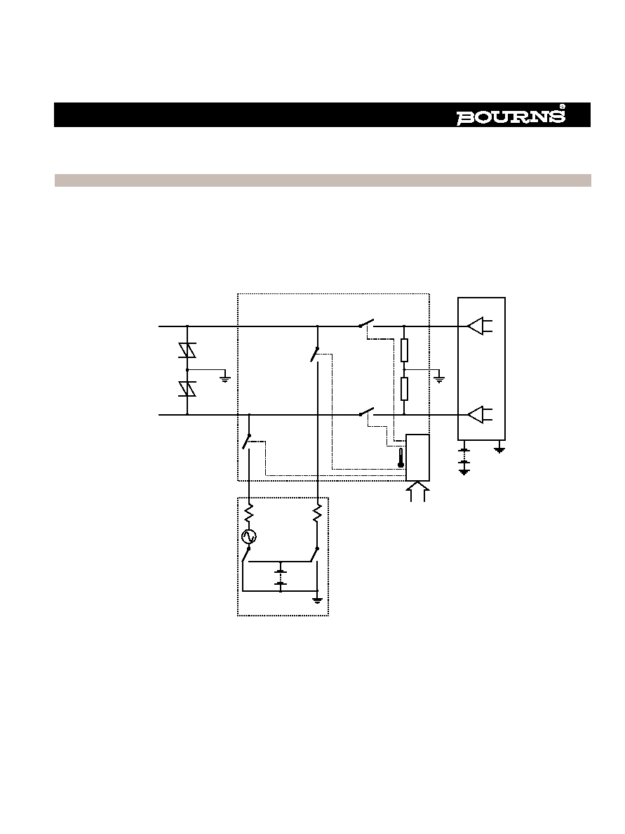
These protector pairs have been designed to limit the peak voltages on the line terminals of `7581/7582/7583 LCAS (Line Card Access Switch)
parts. An LCAS may also be referred to as a Solid-State Relay, SSR, i.e. a replacement of the conventional electro-mechanical relay.
The `7581 LCAS has two solid-state switches which connect the telephone line to the line card SLIC (Subscriber Line Interface Circuit), Figure
12, SW1 and SW2. A further two solid-state switches connect the telephone ringing generator to the line, Figure 12, SW3 and SW4. Applied
5-volt logic signals control the condition of the switches to perform the functions of line disconnect, connection to the SLIC and application of
ringing. If excessive long-term overdissipation occurs, a thermal sensor activates thermal shutdown and opens the switches. The SLIC side of
switches SW1 and SW2 is limited in voltage by internal protectors Th3 and Th4. The line-side of the LCAS is voltage limited by the two TISP
Æ
parts.
Figure 12. Basic LCAS Arrangement
RING
RELAY
SLIC
RELAY
RING
GENERATOR
SW5b
SW5a
R1
R2
V
BAT
V
RING
Th1
Th2
Th3
Th4
SLIC
V
bat
TISP4125M3
OR
TISP4125H3
RING
TIP
SW3
SW4
SW1
SW2
CONTROL
LOGI
C
LCAS
TISP4219M3
OR
TISP4219H3
AI4XAQ
Additional functions are provided by the `7582 (line test access) and the `7583 (test-in and test-out access). Up to three conventional electro-
mechanical relays may be replaced by the LCAS. The resulting size reduction can double the line density of a line card.
This document covers the types of overvoltage protection required by the '7581 LCAS and how the TISP
Æ
part voltages are selected to
provide these requirements. The LCAS '7582 and '7583 are also covered as the additional switches used in these parts are similar to the
'7581.

Specifications are subject to change without notice.
196
JUNE 2001
TISP4xxxH3/M3BJ Series for LCAS Protection
LCAS Switch Ratings
Equivalent Circuit
Figure 13 shows the LCAS switch voltage ratings as breakdown diodes, which must not be allowed to conduct. Each switch has three diodes;
one between poles and the other two from each pole to ground. At 25
∞C, switches SW1 through to SW3 have breakdown diode voltages of
±320 V. Switch SW4 has breakdown diode voltage values of ±465 V for the one between poles and ±320 V for the two diodes connected to
ground. Note that only protection to ground is required, as in the limit, the inter-switch voltage limitation of
±640 V is the same as the switch to
ground limitation of +320 V and -320 V in both polarities.
When a switch is in the off state, the maximum withstand voltage may be set by the switch itself or by the control line to the switch. At 25
∞C,
the switch terminal to ground voltage rating for all the switches is
±320 V. Switches SW1 to SW3 are bidirectional MOS types and can
withstand
±320 V between terminals. Switch SW4 is a bidirectional thyristor which is rated at ±465 V between terminals.
Overcurrents as well as overvoltages occur on telephone lines. In the on state, the thyristor switch, SW4, is capable of withstanding high levels
of current overload. For currents above about 200 mA, the MOS switches, SW1 to SW3, will go into a current limited condition. This will cause
the voltage to rise across the switch and large amounts of power to be developed. In the longer term, this power loss increases the overall chip
temperature. When the temperature exceeds about 125
∞C, thermal shutdown occurs and the switches are set to the off state. Without power
loss, the LCAS will cool. Eventually, the thermal trip will reset, setting the switches back in the high power loss condition again. The cycle of
temperature increase, thermal shutdown, temperature decrease and switch re-activation will continue until the overcurrent ceases.
Figure 13. LCAS Shown with Switch Breakdown Limits
RING
RELAY
SLIC
RELAY
RING
GENERAT OR
SW5a
SW5b
R1
R2
V
BAT
±
2xV
RING
Th1
Th2
Th3
Th4
SLIC
V
bat
RING
TIP
SW3
SW4
SW1
SW2
CONTROL
LOGI
C
+
2xV
RING
-
2xV
RING
V
BAT
0
RING
WIRE
TIP
WIRE
V
BAT
+
2xV
RING
V
BAT
-
2xV
RING
V
BAT
0
RING
WIRE
TIP
WIRE
GROUND-BACKED RINGING
SW5 AS SHOWN
BATTERY-BACKED RINGING
SW5 OPERATED
OVERCURRE
NT
PROT
E
C
T
I
ON
R1
R2
AI4XAR
TISP4125M3
OR
TISP4125H3
TISP4219M3
OR
TISP4219H3

Specifications are subject to change without notice.
197
JUNE 2001
TISP4xxxH3/M3BJ Series for LCAS Protection
Protector Voltages
Protector working and protection voltage design calculations for the LCAS are described in the IEEE Std. C62.37.1-2000, IEEE Guide for the
Application of Thyristor Surge Protection Devices, pp 40-43. These calculations comprehend:
the temprature variation of LCAS voltage ratings,
increase in protection voltage with ambient temperature rise, long term a.c. heating and under impulse conditions,
decrease in working voltage with ambient temperature fall,
ground-backed and battery-backed ringing configurations (see Figure 13).
These calculation techniques were used to set the TISP
Æ
part voltages. Using these TISP
Æ
parts allows normal system voltage levels of
±100 V
on TIP and
±180 V on RING without clipping at 25 ∞C. At 0 ∞C ambient, these voltage levels become ±97 V on TIP and ±174 V on RING. Under
open circuit line conditions, this means that the peak ringing voltage cannot exceed
±174 V for equipment operation down to 0 ∞C ambient.
Assuming a battery voltage of 48 V
±2.5 V and battery-backed ringing, the maximum peak a.c. ring voltage is 174 V - 50.5 V = 123.5 V or 87 V
rms. The working voltage of
±97 V on TIP is more than half the ±174 V working voltage on RING. As a result, the TIP working voltage does not
represent a limitation for systems where the TIP return resistance is equal or less than the RING source resistance.
For balanced impedance ground-backed ringing, the maximum peak a.c. ring voltage under short line conditions (short between TIP and
RING) is limited by the TIP working voltage of
±97 V. In the negative ring polarity, the limit of the voltage is made up from half the battery
voltage plus half of the peak a.c. ring voltage. The maximum peak a.c. ring voltage is 2 x (97 - 50.5/2) = 143.5 V or 101 V rms.
Line test voltage levels must be considered, whether they be applied by using LCAS switches or separate electro-mechanical relays. For these
TISP
Æ
parts, the applied test voltage should not exceed the lowest working voltage, which is
±97 V.

Specifications are subject to change without notice.
198
JUNE 2001
TISP4xxxH3/M3BJ Series for LCAS Protection
MECHANICAL DATA
Recommended Printed Wiring Footprint
Device Symbolization Code
Devices will be coded as below. As the device parameters are symmetrical, terminal 1 is not identified.
SMB Pad Size
MDXX BIA
2.54
(.100)
2.40
(.09 5)
2.16
(.085)
DIMENSIONS ARE:
MILLIMETERS
(INCHES)
Device
Symbolization
Code
TISP4125H3B J
4125H3
TISP4219H3B J
4219H3
TISP4125M3BJ
4125M3
TISP4219M3BJ
4219M3

Specifications are subject to change without notice.
199
JUNE 2001
MECHANICAL DATA
TISP4xxxH3/M3BJ Series for LCAS Protection
SMBJ (DO-214AA) Plastic Surface Mount Diode Package
This surface mount package consists of a circuit mounted on a lead frame and encapsulated within a plastic compound. The compound will
withstand soldering temperature with no deformation, and circuit performance characteristics will remain stable when operated in high
humidity conditions. Leads require no additional cleaning or processing when used in soldered assembly.
SMB
MDXXBHAA
2. 00 - 2.40
(.079 - .094 )
2
1
Index
Mark
(if needed)
0. 10 - 0. 20
(.004 - .008 )
5. 21 - 5.59
(.20 5 - .220)
1. 96 - 2. 32
(.077 - .091 )
3. 30 - 3. 94
(.13 0 - .155)
4.06 - 4.57
(.16 0 - .180 )
0. 76 - 1.52
(.03 0 - .060)
1. 90 - 2.10
(.07 5 - .083)
DIMENSIONS ARE:
MILLIMETERS
(INCHES)

Specifications are subject to change without notice.
200
JUNE 2001
MECHANICAL DATA
TISP4xxxH3/M3BJ Series for LCAS Protection
Tape Dimensions
SMB Package Single-Sprocket Tape
NOTES: A. The clearance between the component and the cavity must be within 0.05 mm (.002 in) MIN. to 0.65 mm (.026 in)
MAX. so that the component cannot rotate more than 20
∞ within the determined cavity.
B. Taped devices are supplied on a reel of the following dimensions:
Reel
diameter:
330
mm
± 3.0 mm (12.99 in ± .118 in)
Reel hub diameter: 75 mm (2.95 in) MIN.
Reel axial hole:
13.0 mm
± 0.5 mm (.512 in ± .020 in)
C. 3000 devices are on a reel.
MDXXBJA
Direction of Feed
0 MIN .
Carrier Tape
Embossment
Cover
Tape
20
∞
Typical component
cavity center line
Maximium component
rotation
Typical component
center line
Index
Mark
(if needed)
3. 90 - 4.10
(.154 - .161 )
1. 95 - 2.05
(.07 7 - .081 )
1. 55 - 1.65
(.061 - .065 )
MAX .
0. 40
(.01 6)
MAX .
4. 5
(.17 7)
MAX .
8. 20
(.32 3)
11.70 - 12.30
(.461 - .484 )
5. 45 - 5.55
(.215 - .219 )
MIN .
1. 5
(.05 9)
1. 65 - 1.85
(.065 - .073 )
7. 90 - 8.10
(.311 - .319 )