Specifications are subject to change without notice.
1
AUGUST 2001 - REVISED FEBRUARY 2003
TISP4xxxM3AJ Overvoltage Protector Series
TISP4070M3AJ THRU TISP4115M3AJ,
TISP4125M3AJ THRU TISP4220M3AJ,
TISP4240M3AJ THRU TISP4395M3AJ
BIDIRECTIONAL THYRISTOR OVERVOLTAGE PROTECTORS
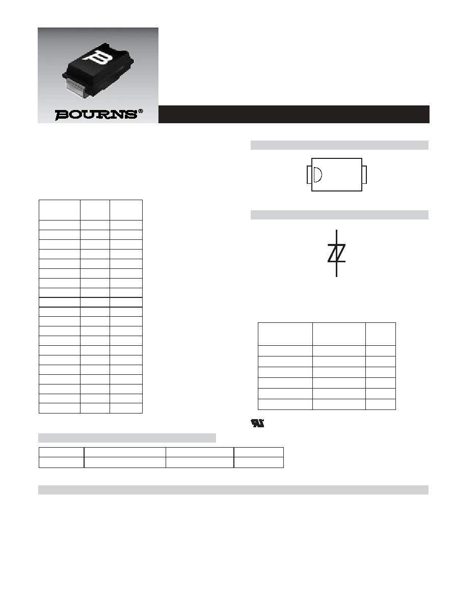
Device Symbol
4 kV 10/700, 100 A 5/310 ITU-T K.20/21 rating
SMA (DO-214AC) Package
25% Smaller Placement Area than SMB
Low Differential Capacitance .......................................... 39 pF
Ion-Implanted Breakdown Region
Precise and Stable Voltage
Low Voltage Overshoot under Surge
SMAJ Package (Top View)
Rated for International Surge Wave Shapes
Device
V
DRM
V
V
(BO)
V
`4070
58
70
`4080
65
80
`4090
68
90
`4095
75
95
`4115
90
115
`4125
100
125
`4145
120
145
`4165
135
165
`4180
145
180
`4200
155
200
`4220
160
220
`4240
180
240
`4250
190
250
`4265
200
265
`4290
220
290
`4300
230
300
`4320
240
320
`4350
275
350
`4360
290
360
`4395
320
395
MDXXCCE
1
2
R (B)
T (A)
Description
These devices are designed to limit overvoltages on the telephone line. Overvoltages are normally caused by a.c. power system or lightning
flash disturbances which are induced or conducted on to the telephone line. A single device provides 2-point protection and is typically used
for the protection of 2-wire telecommunication equipment (e.g. between the Ring and Tip wires for telephones and modems). Combinations of
devices can be used for multi-point protection (e.g. 3-point protection between Ring, Tip and Ground).
The protector consists of a symmetrical voltage-triggered bidirectional thyristor. Overvoltages are initially clipped by breakdown clamping until
the voltage rises to the breakover level, which causes the device to crowbar into a low-voltage on state. This low-voltage on state causes the
current resulting from the overvoltage to be safely diverted through the device. The high crowbar holding current prevents d.c. latchup as the
diverted current subsides.
How To Order
Device
Package
Carrier
Order As
TISP 4xxxM3AJ AJ (J-Bend DO-214AC/SMA) Embossed Tape Reeled TISP4xxxM3AJR
Insert xxx value corresponding to protection voltages of 070, 080, 095, etc.
T
R
SD4XAA
T
erminals T and R correspond to the
alternative line designators of A and B
Wave Shape
Standard
I
TSP
A
2/10 �s
GR-1089-CORE
300
8/20 �s
IEC 61000-4-5
220
10/160 �s
FCC Part 68
120
10/700 �s
ITU-T K.20/21/45
100
10/560 �s
FCC Part 68
75
10/1000 �s
GR-1089-CORE
50
............................................ UL Recognized Components

Specifications are subject to change without notice.
2
AUGUST 2001 - REVISED FEBRUARY 2003
The TISP4xxxM3AJ range consists of twenty voltage variants to meet various maximum system voltage levels (58 V to 320 V). They are
guaranteed to voltage limit and withstand the listed international lightning surges in both polarities. These medium (M) current protection
devices are in a plastic package SMAJ (JEDEC DO-214AC with J-bend leads) and supplied in embossed tape reel pack. For alternative
voltage and holding current values, consult the factory. For higher rated impulse currents, the 100 A 10/1000 TISP4xxxH3BJ series in the SMB
(JEDEC DO-214AA) package is available.
TISP4xxxM3AJ Overvoltage Protector Series
Description (continued)
Absolute Maximum Ratings, TA = 25 �C (Unless Otherwise Noted)
Rating
Symbol
Value
Unit
Repetitive peak off-state voltage, (see Note 1)
`4070
`4080
`4095
`4115
`4125
`4145
`4165
`4180
`4200
`4220
`4240
`4250
`4265
`4290
`4300
`4350
`4360
`4395
V
DRM
� 58
� 65
`4090
� 68
� 75
� 90
�100
�120
�135
�145
�155
�160
�180
�190
�200
�220
�230
`4320
�240
�275
�290
�320
V
Non-repetitive peak on-state pulse current (see Notes 2, 3 and 4)
I
TSP
A
2/10 �s (GR-1089-CORE, 2/10 �s voltage wave shape)
300
8/20 �s (IEC 61000-4-5, combination wave generator, 1.2/50 voltage, 8/20 current)
220
10/160 �s (FCC Part 68, 10/160 �s voltage wave shape)
120
5/200 �s (VDE 0433, 10/700 �s voltage wave shape)
110
0.2/310 �s (I3124, 0.5/700 �s voltage wave shape)
100
5/310 �s (ITU-T K.20/21/45, K.44 10/700 �s voltage wave shape)
100
5/310 �s (FTZ R12, 10/700 �s voltage wave shape)
100
10/560 �s (FCC Part 68, 10/560 �s voltage wave shape)
75
10/1000 �s (GR-1089-CORE, 10/1000 �s voltage wave shape)
50
Non-repetitive peak on-state current (see Notes 2, 3 and 5)
I
TSM
23
24
1.6
A
20 ms (50 Hz) full sine wave
16.7 ms (60 Hz) full sine wave
1000 s 50 Hz/60 Hz a.c.
Initial rate of rise of on-state current,
Exponential current ramp, Maximum ramp value < 100 A
di
T
/dt
300
A/�s
Junction temperature
T
J
-40 to +150
�C
Storage temperature range
T
stg
-65 to +150
�C
NOTES: 1. See Applications Information and Figure 10 for voltage values at lower temperatures.
2. Initially, the TISP4xxxM3AJ must be in thermal equilibrium with T
J
= 25 �C.
3. The surge may be repeated after the TISP4xxxM3AJ returns to its initial conditions.
4. See Applications Information and Figure 11 for current ratings at other temperatures.
5. EIA/JESD51-2 environment and EIA/JESD51-3 PCB with standard footprint dimensions connected with 5 A rated printed wiring
track widths. See Figure 9 for the current ratings at other durations. Derate current values at -0.61 %/�C for ambient temperatures
above 25 � C.

Specifications are subject to change without notice.
3
AUGUST 2001 - REVISED FEBRUARY 2003
TISP4xxxM3AJ Overvoltage Protector Series
Electrical Characteristics, TA = 25 �C (Unless Otherwise Noted)
Parameter
Test Conditions
Min
Typ
Max
Unit
I
DRM
Repetitive peak off-
state current
V
D
= V
DRM
T
A
= 25 �C
T
A
= 85 �C
�5
�10
�A
V
(BO)
Breakover voltage
dv/dt = �250 V/ms, R
SOURCE
= 300
`4070
`4080
`4095
`4115
`4125
`4145
`4165
`4180
`4200
`4220
`4240
`4250
`4265
`4290
`4300
`4350
`4360
`4395
�70
�80
`4090
�90
�95
�115
�125
�145
�165
�180
�200
�220
�240
�250
�265
�290
�300
`4320
�320
�350
�360
�395
V
V
(BO)
Impulse breakover
voltage
dv/dt �1000 V/�s, Linear voltage ramp,
Maximum ramp value = �500 V
di/dt = �20 A/�s, Linear current ramp,
Maximum ramp value = �10 A
`4070
`4080
`4095
`4115
`4125
`4145
`4165
`4180
`4200
`4220
`4240
`4250
`4265
`4290
`4300
`4350
`4360
`4395
�78
�88
`4090
�98
�102
�122
�132
�151
�171
�186
�207
�227
�247
�257
�272
�298
�308
`4320
�328
�359
�370
�405
V
I
(BO)
Breakover current
dv/dt = �250 V/ms, R
SOURCE
= 300
�0.15
�0.6
A
V
T
On-state voltage
I
T
= �5 A, t
W
= 100 �s
�3
V
I
H
Holding current
I
T
= �5 A, di/dt = +/-30 mA/ms
�0.15
�0.35
A
dv/dt
Critical rate of rise of
off-state voltage
Linear voltage ramp, Maximum ramp value < 0.85V
DRM
�5
kV/�s

Specifications are subject to change without notice.
4
AUGUST 2001 - REVISED FEBRUARY 2003
Thermal Characteristics
TISP4xxxM3AJ Overvoltage Protector Series
Electrical Characteristics, TA = 25 �C (Unless Otherwise Noted)
C
off
Off-state capacitance
f = 1 MHz,
V
d
= 1 V rms, V
D
= 0,
f = 1 MHz,
V
d
= 1 V rms, V
D
= -1 V
f = 1 MHz,
V
d
= 1 V rms, V
D
= -2 V
f = 1 MHz,
V
d
= 1 V rms, V
D
= -50 V
f = 1 MHz,
V
d
= 1 V rms, V
D
= -100 V
(see Note 6)
4070 thru `4115
`4125 thru `4220
`4240 thru `4400
`4070 thru `4115
`4125 thru `4220
`4240 thru `4395
`4070 thru `4115
`4125 thru `4220
`4240 thru `4395
`4070 thru `4115
`4125 thru `4220
`4240 thru `4400
`4125 thru `4220
`4240 thru `4395
83
62
50
78
56
45
72
52
42
36
26
19
21
15
100
74
60
94
67
54
87
62
50
44
31
22
25
18
pF
NOTE
6: To avoid possible voltage clipping, the `4125 is tested with V
D
= -98 V.
Parameter
Test Conditions
Min
Typ
Max
Unit
A
I
D
Off-state current
V
D
= �50 V
T
A
= 85 �C
�10
�
Parameter
Test Conditions
Min
Typ
Max
Unit
R
JA
Junction to free air thermal resistance
EIA/JESD51-3 PCB, I
T
= I
TSM(1000)
,
T
A
= 25 �C, (see Note 7)
115
�C/W
265 mm x 210 mm populated line card,
4-layer PCB, I
T
= I
TSM(1000)
, T
A
= 25 �C
52
NOTE
7: EIA/JESD51-2 environment and PCB has standard footprint dimensions connected with 5 A rated printed wiring track widths.
Specifications are subject to change without notice.
5
AUGUST 2001 - REVISED FEBRUARY 2003
TISP4xxxM3AJ Overvoltage Protector Series
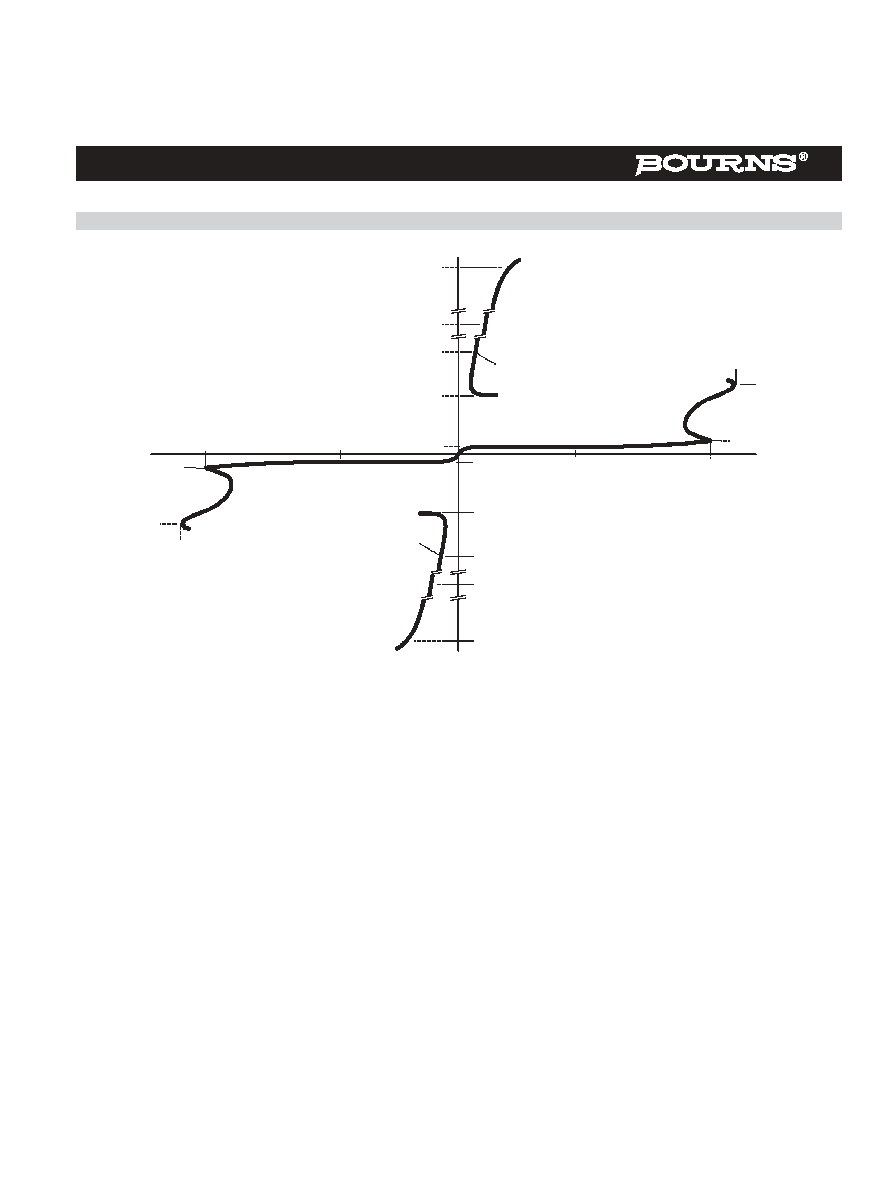
Parameter Measurement Information
Figure 1. Voltage-Current Characteristic for T and R Terminals
All Measurements are Referenced to the R Terminal
-v
V
DRM
I
DRM
V
D
I
H
I
T
V
T
I
TSM
I
TSP
V
(BO)
I
(BO)
I
D
Quadrant I
I
Switching
Characteristic
+v
+i
V
(BO)
I
(BO)
V
D
I
D
I
H
I
T
V
T
I
TSM
I
TSP
-i
Quadrant III
Switching
Characteristic
PMXXAAB
V
DRM
I
DRM