
TISP4072F3LM, TISP4082F3LM, TISP4125F3LM, TISP4150F3LM, TISP4180F3LM
TISP4240F3LM, TISP4260F3LM, TISP4290F3LM, TISP4320F3LM, TISP4380F3LM
BIDIRECTIONAL THYRISTOR OVERVOLTAGE PROTECTORS
P R O D U C T I N F O R M A T I O N
1
DECEMBER 1998 - REVISED APRIL 1999
Copyright © 1999, Power Innovations Limited, UK
Information is current as of publication date. Products conform to specifications in accordance
with the terms of Power Innovations standard warranty. Production processing does not
necessarily include testing of all parameters.
TELECOMMUNICATION SYSTEM SECONDARY PROTECTION
q
Ion-Implanted Breakdown Region
Precise and Stable Voltage
Low Voltage Overshoot under Surge
q
Rated for International Surge Wave Shapes
q
Ordering Information
DEVICE
V
DRM
V
V
(BO)
V
`4072
58
72
`4082
66
82
`4125
100
125
`4150
120
150
`4180
145
180
`4240
180
240
`4260
200
260
`4290
220
290
`4320
240
320
`4380
270
380
WAVE SHAPE
STANDARD
I
TSP
A
10/160 µs
FCC Part 68
60
0.5/700 µs
I3124
38
10/700 µs
ITU-T K20/21
50
10/560 µs
FCC Part 68
45
10/1000 µs
REA PE-60
35
DEVICE TYPE
PACKAGE TYPE
TISP4xxxF3LM
Straight Lead DO-92 Bulk Pack
TISP4xxxF3LMR
Straight Lead DO-92 Tape and Reeled
TISP4xxxF3LMFR
Formed Lead DO-92 Tape and Reeled
description
These devices are designed to limit overvoltages on the telephone line. Overvoltages are normally caused by
a.c. power system or lightning flash disturbances which are induced or conducted on to the telephone line. A
single device provides 2-point protection and is typically used for the protection of 2-wire telecommunication
equipment (e.g. between the Ring to Tip wires for telephones and modems). Combinations of devices can be
used for multi-point protection (e.g. 3-point protection between Ring, Tip and Ground).
The protector consists of a symmetrical voltage-triggered bidirectional thyristor. Overvoltages are initially
clipped by breakdown clamping until the voltage rises to the breakover level, which causes the device to
crowbar into a low-voltage on state. This low-voltage on state causes the current resulting from the
overvoltage to be safely diverted through the device. The high crowbar holding current prevents d.c. latchup
as the diverted current subsides.
This TISP4xxxF3LM range consists of ten voltage variants to meet various maximum system voltage levels
(58 V to 270 V). They are guaranteed to voltage limit and withstand the listed international lightning surges in
both polarities. These protection devices are supplied in a DO-92 (LM) cylindrical plastic package. The
device symbol
LMF PACKAGE
(LM PACKAGE WITH FORMED LEADS)
(TOP VIEW)
NC - No internal connection on pin 2
NC
T(A)
R(B)
MD4XAKB
1
2
3
LM PACKAGE
(TOP VIEW)
NC - No internal connection on pin 2
NC
T(A)
R(B)
MD4XAT
1
2
3
T
R
SD4XAA
Terminals T and R correspond to the
alternative line designators of A and B

TISP4072F3LM, TISP4082F3LM, TISP4125F3LM, TISP4150F3LM, TISP4180F3LM
TISP4240F3LM, TISP4260F3LM, TISP4290F3LM, TISP4320F3LM, TISP4380F3LM
BIDIRECTIONAL THYRISTOR OVERVOLTAGE PROTECTORS
2
DECEMBER 1998 - REVISED APRIL 1999
P R O D U C T I N F O R M A T I O N
TISP4xxxF3LM is a straight lead DO-92 supplied in bulk pack and on tape and reeled. The TISP4xxxF3LMF
is a formed lead DO-92 supplied only on tape and reeled.
NOTES: 1. Initially the TISP must be in thermal equilibrium with 0 ∞C < T
J
< 70 ∞C.
2. The surge may be repeated after the TISP returns to its initial conditions.
3. Above 70 ∞C, derate linearly to zero at 150 ∞C lead temperature.
absolute maximum ratings
RATING
SYMBOL
VALUE
UNIT
Repetitive peak off-state voltage (0 ∞C < T
J
< 70 ∞C)
`4072
`4082
`4125
`4150
`4180
`4240
`4260
`4290
`4320
`4380
V
DRM
± 58
± 66
± 100
± 120
± 145
± 180
± 200
± 220
± 240
± 270
V
Non-repetitive peak on-state pulse current (see Notes 1, 2 and 3)
I
TSP
A
2/10 µs (FCC Part 68, 2/10 µs voltage wave shape) excluding `4072 - `4082
175
8/20 µs (ANSI C62.41, 1.2/50 µs voltage wave shape) excluding `4072 - `4082
120
10/160 µs (FCC Part 68, 10/160 µs voltage wave shape)
60
5/200 µs (VDE 0433, 2 kV, 10/700 µs voltage wave shape)
50
0.2/310 µs (I3124, 1.5 kV, 0.5/700 µs voltage wave shape)
38
5/310 µs (ITU-T K20/21, 1.5 kV, 10/700 µs voltage wave shape)
38
5/310 µs (FTZ R12, 2 kV, 10/700 µs voltage wave shape)
50
10/560 µs (FCC Part 68, 10/560 µs voltage wave shape)
45
10/1000 µs (REA PE-60, 10/1000 µs voltage wave shape)
35
2/10 µs (FCC Part 68, 2/10 µs voltage wave shape) `4072 - `4082 only
80
8/20 µs (ANSI C62.41, 1.2/50 µs voltage wave shape) `4072 - `4082 only
70
Non-repetitive peak on-state current (see Notes 2 and 3)
I
TSM
4
A
50/60 Hz,
1 s
Initial rate of rise of on-state current,
Linear current ramp, Maximum ramp value < 38 A
di
T
/dt
250
A/µs
Junction temperature
T
J
-40 to +150
∞C
Storage temperature range
T
stg
-55 to +150
∞C
description (continued)

3
DECEMBER 1998 - REVISED APRIL 1999
TISP4072F3LM, TISP4082F3LM, TISP4125F3LM, TISP4150F3LM, TISP4180F3LM
TISP4240F3LM, TISP4260F3LM, TISP4290F3LM, TISP4320F3LM, TISP4380F3LM
BIDIRECTIONAL THYRISTOR OVERVOLTAGE PROTECTORS
P R O D U C T I N F O R M A T I O N
electrical characteristics for the T and R terminals, T
J
= 25 ∞C (unless otherwise noted)
PARAMETER
TEST CONDITIONS
MIN
TYP
MAX
UNIT
I
DRM
Repetitive peak off-
state current
V
D
= ±V
DRM
, 0 ∞C < T
J
< 70 ∞C
±10
µA
V
(BO)
Breakover voltage
dv/dt = ±250 V/ms,
R
SOURCE
= 300
`4072
`4082
`4125
`4150
`4180
`4240
`4260
`4290
`4320
`4380
±72
±82
±125
±150
±180
±240
±260
±290
±320
±380
V
V
(BO)
Impulse breakover
voltage
dv/dt = ±1000 V/µs,
R
SOURCE
= 50
,
di/dt < 20 A/µs
`4072
`4082
`4125
`4150
`4180
`4240
`4260
`4290
`4320
`4380
±86
±96
±143
±168
±198
±267
±287
±317
±347
±407
V
I
(BO)
Breakover current
dv/dt = ±250 V/ms,
R
SOURCE
= 300
±0.15
±0.6
A
V
T
On-state voltage
I
T
= ±5 A, t
W
= 100 µs
±3
V
I
H
Holding current
I
T
= ±5 A, di/dt = +/-30 mA/ms
±0.15
A
dv/dt
Critical rate of rise of
off-state voltage
Linear voltage ramp, Maximum ramp value < 0.85V
DRM
±5
kV/µs
I
D
Off-state current
V
D
= ±50 V
±10
µA
C
off
Off-state capacitance
f = 100 kHz,
V
d
= 1 Vrms, V
D
= 0,
f = 100 kHz,
V
d
= 1 Vrms, V
D
= -50 V
`4072 - `4082
`4125 - `4180
`4240 - `4380
`4072 - `4082
`4125 - `4180
`4240 - `4380
63
43
44
25
15
11
108
74
74
40
25
20
pF
thermal characteristics
PARAMETER
TEST CONDITIONS
MIN
TYP
MAX
UNIT
R
JA
Junction to free air thermal resistance
EIA/JESD51-3 PCB mounted in an EIA/
JESD51-2 enclosure
120
∞C/W

TISP4072F3LM, TISP4082F3LM, TISP4125F3LM, TISP4150F3LM, TISP4180F3LM
TISP4240F3LM, TISP4260F3LM, TISP4290F3LM, TISP4320F3LM, TISP4380F3LM
BIDIRECTIONAL THYRISTOR OVERVOLTAGE PROTECTORS
4
DECEMBER 1998 - REVISED APRIL 1999
P R O D U C T I N F O R M A T I O N
PARAMETER MEASUREMENT INFORMATION
Figure 1. VOLTAGE-CURRENT CHARACTERISTIC FOR R AND T TERMINALS
ALL MEASUREMENTS ARE REFERENCED TO THE T TERMINAL
-v
V
DRM
I
DRM
V
D
I
H
I
T
V
T
I
TSM
I
TSP
V
(BO)
I
(BO)
I
D
Quadrant I
Switching
Characteristic
+v
+i
V
(BO)
I
(BO)
V
DRM
I
DRM
V
D
I
D
I
H
I
T
V
T
I
TSM
I
TSP
-i
Quadrant III
Switching
Characteristic
PMXXAAB
5
DECEMBER 1998 - REVISED APRIL 1999
TISP4072F3LM, TISP4082F3LM, TISP4125F3LM, TISP4150F3LM, TISP4180F3LM
TISP4240F3LM, TISP4260F3LM, TISP4290F3LM, TISP4320F3LM, TISP4380F3LM
BIDIRECTIONAL THYRISTOR OVERVOLTAGE PROTECTORS
P R O D U C T I N F O R M A T I O N
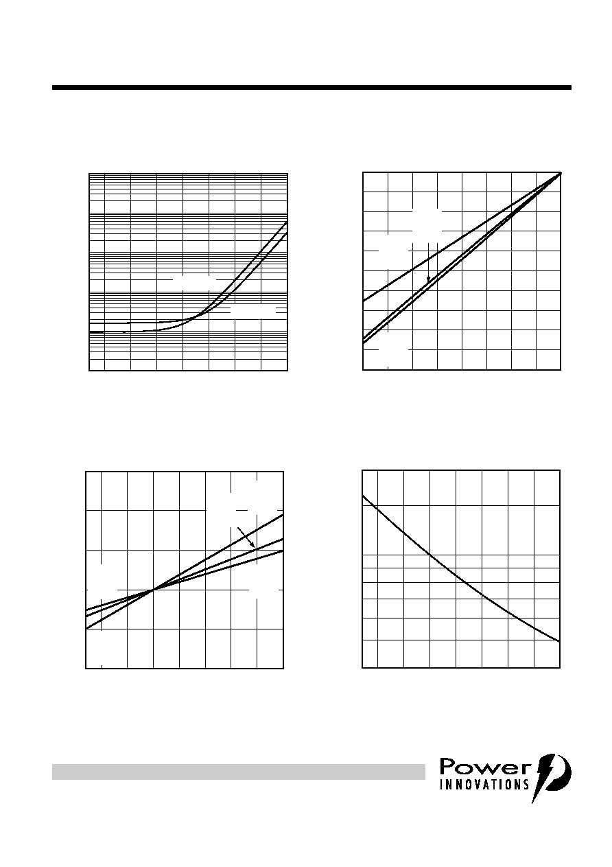
TYPICAL CHARACTERISTICS
Figure 2.
Figure 3.
Figure 4.
Figure 5.
OFF-STATE CURRENT
vs
JUNCTION TEMPERATURE
T
J
- Junction Temperature - ∞C
-25
0
25
50
75
100
125
150
I
D
-
O
f
f-
S
t
ate Current -
µ
A
0∑001
0∑01
0∑1
1
10
100
TC4XAA
V
D
= -50 V
V
D
= 50 V
V
DRM
DERATING FACTOR
vs
MINIMUM AMBIENT TEMPERATURE
T
AMIN
- Minimum Ambient Temperature - ∞C
-40
-35
-30
-25
-20
-15
-10
-5
0
D
e
r
a
t
i
ng Fact
o
r
0.95
0.96
0.97
0.98
0.99
1.00
TC4XAB
'4125
THRU
'4180
'4072
AND
'4082
'4240
THRU
'4380
ON-STATE CURRENT
vs
ON-STATE VOLTAGE
V
T
- On-State Voltage - V
2
3
4
5
6
7 8 9
1
10
I
T
-
On
-Sta
te Cu
rren
t
-
A
1
10
100
TC3MAL
-40∞C
150∞C
25∞C
NORMALISED V
(BO)
vs
AMBIENT TEMPERATURE
T
A
- Ambient Temperature - ∞C
-25
0
25
50
75
100
125
150
V
(BO
)
N
o
r
m
al
i
sed t
o
25∞
C
V
a
l
u
e
0.9
1.0
1.1
TC4XAC
'4240
THRU
'4380
'4072
AND
'4082
'4125
THRU
'4180
'4240
THRU
'4380
'4072
AND
'4082
NORMALISED HOLDING CURRENT
vs
JUNCTION TEMPERATURE
T
J
- Junction Temperature - ∞C
-25
0
25
50
75
100
125
150
N
o
r
m
a
lis
ed H
o
ldin
g Cur
r
e
nt
0.4
0.5
0.6
0.7
0.8
0.9
1.5
2.0
1.0
TC4XAD