
Specifications are subject to change without notice.
NOVEMBER 1997 - REVISED DECEMBER 2001
TISP4xxxM3LM Overvoltage Protector Series
TISP4070M3LM THRU TISP4115M3LM,
TISP4125M3LM THRU TISP4220M3LM,
TISP4240M3LM THRU TISP4400M3LM
BIDIRECTIONAL THYRISTOR OVERVOLTAGE PROTECTORS
Summary Current Ratings
Summary Electrical Characteristics
TISP4xxxM3LM Overview
This TISPÆ device series protects central office, access and customer premise equipment against overvoltages on the telecom line. The
TISP4xxxM3LM is available in a wide range of voltages and has a medium current capability. These protectors have been specified mindful of
the following standards and recommendations: GR-1089-CORE, FCC Part 68, UL1950, EN 60950, IEC 60950, ITU-T K.20, K.21 and K.45. The
TISP4350M3LM meets the FCC Part 68 "B" ringer voltage requirement and survives the Type B impulse tests. These devices are housed in a
through-hole DO-92 package (TO-92 package with cropped center leg).
Part #
V
DRM
V
V
(BO)
V
V
T
@ I
T
V
I
DRM
µA
I
(BO)
mA
I
T
A
I
H
mA
C
o
@ -2 V
pF
Functionally
Replaces
TISP4070M3
58
70
3
5
600
5
150
120
P0640EA
TISP4080M3
65
80
3
5
600
5
150
120
P0720EA
TISP4095M3
75
95
3
5
600
5
150
120
P0900EA
TISP4115M3
90
115
3
5
600
5
150
120
P1100EA
TISP4125M3
100
125
3
5
600
5
150
65
TISP4145M3
120
145
3
5
600
5
150
65
P1300EA
TISP4165M3
135
165
3
5
600
5
150
65
TISP4180M3
145
180
3
5
600
5
150
65
P1500EA
TISP4220M3
160
220
3
5
600
5
150
65
P1800EA
TISP4240M3
180
240
3
5
600
5
150
55
TISP4250M3
190
250
3
5
600
5
150
55
P2300EA
TISP4260M3
200
260
3
5
600
5
150
55
TISP4290M3
220
290
3
5
600
5
150
55
P2600EA
TISP4300M3
230
300
3
5
600
5
150
55
TISP4350M3
275
350
3
5
600
5
150
55
P3100EA
TISP4395M3
320
395
3
5
600
5
150
55
P3500EA
TISP4400M3
300
400
3
5
600
5
150
55
Bourns' part has an improved protection voltage
Parameter
I
TSP
A
I
TSM
A
di/dt
A/µs
Waveshape
2/10
1.2/50, 8/20
10/160
5/320
10/560
10/1000
1 cycle 60 Hz
2/10 Wavefront
Value
300
220
120
100
75
50
32
300

Specifications are subject to change without notice.
NOVEMBER 1997 - REVISED DECEMBER 2001
T
R
SD4XAA
Terminals T and R correspond to the
alternative line designators of A and B
LMF Package (LM Package with Formed Leads) (Top View)
Device
V
DRM
V
V
(BO)
V
`4070
58
70
`4080
65
80
`4095
75
95
`4115
90
115
`4125
100
125
`4145
120
145
`4165
135
165
`4180
145
180
`4220
160
220
`4240
180
240
`4250
190
250
`4260
200
260
`4290
220
290
`4300
230
300
`4350
275
350
`4395
320
395
`4400
300
400
Waveshape
Standard
I
TSP
A
2/10 µs
GR-1089-CORE
300
8/20 µs
IEC 61000-4-5
220
10/160 µs
FCC Part 68
120
10/700 µs
ITU-T K.20/21
FCC Part 68
100
10/560 µs
FCC Part 68
75
10/1000 µs
GR-1089-CORE
50
How To Order
LM Package (Top View)
Ion-Implanted Breakdown Region
Precise and Stable Voltage
Low Voltage Overshoot under Surge
Rated for International Surge Wave Shapes
Device Symbol
Device
Package
Carrier
Order As
TISP4xxxM3LM
Straight Lead DO-92 (LM)
Bulk Pack
TISP4xxxM3LM
Tape and Reeled
TISP4xxxM3LMR
Formed Lead DO-92 (LMF)
Tape and Reeled TISP4xxxM3LMFR
Insert xxx value corresponding to protection voltages of 070, 080, 095, 115 etc.
Description
TISP4xxxM3LM Overvoltage Protector Series
ITU-T K.20/21 Rating ...........................4 kV 10/700,100 A 5/310
These devices are designed to limit overvoltages on the telephone line. Overvoltages are normally caused by a.c. power system or lightning
flash disturbances which are induced or conducted on to the telephone line. A single device provides 2-point protection and is typically used
for the protection of 2-wire telecommunication equipment (e.g. between the Ring and Tip wires for telephones and modems). Combinations of
devices can be used for multi-point protection (e.g. 3-point protection between Ring, Tip and Ground).
Low Differential Capacitance .................................. 43 pF max.
.............................................. UL Recognized Component
NC - No internal connection on pin 2
NC
T(A)
R(B)
MD4XAT
1
2
3
NC - No internal connection on pin 2
NC
T(A)
R(B)
MD4XAKB
1
2
3

Specifications are subject to change without notice.
NOVEMBER 1997 - REVISED DECEMBER 2001
Description (continued)
TISP4xxxM3LM Overvoltage Protector Series
Rating
Symbol
Value
Unit
Repetitive peak off-state voltage, (see Note 1)
`4070
`4080
`4095
`4115
`4125
`4145
`4165
`4180
`4220
`4240
`4250
`4260
`4290
`4300
`4350
`4395
`4400
V
DRM
± 58
± 65
± 75
± 90
±100
±120
±135
±145
±160
±180
±190
±200
±220
±230
±275
±320
±300
V
Non-repetitive peak on-state pulse current (see Notes 2, 3 and 4)
I
TSP
A
2/10 µs (GR-1089-CORE, 2/10 µs voltage wave shape)
300
8/20 µs (IEC 61000-4-5, combination wave generator, 1.2/50 voltage, 8/20 current)
220
10/160 µs (FCC Part 68, 10/160 µs voltage wave shape)
120
5/200 µs (VDE 0433, 10/700 µs voltage wave shape)
110
0.2/310 µs (I 31-24, 0.5/700 µs voltage wave shape)
100
5/310 µs (ITU-T K.20/21, 10/700 µs voltage wave shape)
100
5/310 µs (FTZ R12, 10/700 µs voltage wave shape)
100
5/320 µs (FCC Part 68, 9/720 µs voltage wave shape)
100
10/560 µs (FCC Part 68, 10/560 µs voltage wave shape)
75
10/1000 µs (GR-1089-CORE, 10/1000 µs voltage wave shape)
50
Non-repetitive peak on-state current (see Notes 2, 3 and 5)
I
TSM
30
32
2.1
A
20 ms (50 Hz) full sine wave
16.7 ms (60 Hz) full sine wave
1000 s 50 Hz/60 Hz a.c.
Initial rate of rise of on-state current,
Exponential current ramp, Maximum ramp value < 100 A
di
T
/dt
300
A/µs
Junction temperature
T
J
-40 to +150
∞C
Storage temperature range
T
stg
-65 to +150
∞C
NOTES: 1. See Applications Information and Figure 10 for voltage values at lower temperatures.
2. Initially the TISP4xxxM3LM must be in thermal equilibrium with T
J
= 25 ∞C.
3. The surge may be repeated after the TISP4xxxM3LM returns to its initial conditions.
4. See Applications Information and Figure 11 for current ratings at other temperatures.
5. EIA/JESD51-2 environment and EIA/JESD51-3 PCB with standard footprint dimensions connected with 5 A rated printed wiring
track widths. See Figure 8 for the current ratings at other durations. Derate current values at -0.61 %/∞C for ambient
temperatures above 25 ∞C
Absolute Maximum Ratings, TA = 25 ∞C (Unless Otherwise Noted)
The protector consists of a symmetrical voltage-triggered bidirectional thyristor. Overvoltages are initially clipped by breakdown clamping until
the voltage rises to the breakover level, which causes the device to crowbar into a low-voltage on state. This low-voltage on state causes the
current resulting from the overvoltage to be safely diverted through the device. The high crowbar holding current prevents d.c. latchup as the
diverted current subsides.
This TISP4xxxM3LM range consists of seventeen voltage variants to meet various maximum system voltage levels (58 V to 320 V). They are
guaranteed to voltage limit and withstand the listed international lightning surges in both polarities. These protection devices are supplied in a
DO-92 (LM) cylindrical plastic package. The TISP4xxxM3LM is a straight lead DO-92 supplied in bulk pack and on tape and reel. The
TISP4xxxM3LMF is a formed lead DO-92 supplied only on tape and reel. For higher rated impulse currents in the DO-92 package, the 100 A
10/1000 TISP4xxxH3LM series is available.

Specifications are subject to change without notice.
NOVEMBER 1997 - REVISED DECEMBER 2001
Parameter
Test Conditions
Min
Typ
Max
Unit
I
DRM
Repetitive peak off-
state current
V
D
= ±V
DRM
T
A
= 25 ∞C
T
A
= 85 ∞C
±5
±10
µA
V
(BO)
Breakover voltage
dv/dt = ±750 V/ms, R
SOURCE
= 300
`4070
`4080
`4095
`4115
`4125
`4145
`4165
`4180
`4220
`4240
`4250
`4260
`4290
`4300
`4350
`4395
`4400
±70
±80
±95
±115
±125
±145
±165
±180
±220
±240
±250
±260
±290
±300
±350
±395
±400
V
V
(BO)
Impulse breakover
voltage
dv/dt
±1000 V/µs, Linear voltage ramp,
Maximum ramp value = ±500 V
di/dt = ±20 A/µs, Linear current ramp,
Maximum ramp value = ±10 A
`4070
`4080
`4095
`4115
`4125
`4145
`4165
`4180
`4220
`4240
`4250
`4260
`4290
`4300
`4350
`4395
`4400
±78
±88
±102
±122
±132
±151
±171
±186
±227
±247
±257
±267
±298
±308
±359
±405
±410
V
I
(BO)
Breakover current
dv/dt = ±750 V/ms, R
SOURCE
= 300
±0.15
±0.6
A
V
T
On-state voltage
I
T
= ±5 A, t
W
= 100 µs
±3
V
I
H
Holding current
I
T
= ±5 A, di/dt = - /+ 3 0 mA/ms
±0.15
±0.6
A
dv/dt
Critical rate of rise of
off-state voltage
Linear voltage ramp, Maximum ramp value < 0.85V
DRM
±5
kV/µs
I
D
Off-state current
V
D
= ±50 V
T
A
= 85 ∞C
±10
µA
Electrical Characteristics, TA = 25 ∞C (Unless Otherwise Noted)
TISP4xxxM3LM Overvoltage Protector Series

Specifications are subject to change without notice.
NOVEMBER 1997 - REVISED DECEMBER 2001
Parameter
Test Conditions
Min
Typ
Max
Unit
R
JA
Junction to free air thermal resistance
EIA/JESD51-3 PCB, I
T
= I
TSM(1000)
,
T
A
= 25 ∞C, (see Note 7)
120
∞C/W
265 mm x 210 mm populated line card,
4-layer PCB, I
T
= I
TSM(1000)
, T
A
= 25 ∞C
57
NOTE
7: EIA/JESD51-2 environment and PCB has standard footprint dimensions connected with 5 A rated printed wiring track widths.
Thermal Characteristics
TISP4xxxM3LM Overvoltage Protector Series
Electrical Characteristics, TA = 25 ∞C (Unless Otherwise Noted) (continued)
C
off
Off-state capacitance
f = 100 kHz,
V
d
= 1 V rms, V
D
= 0,
f = 100 kHz,
V
d
= 1 V rms, V
D
= -1 V
f = 100 kHz,
V
d
= 1 V rms, V
D
= -2 V
f = 100 kHz,
V
d
= 1 V rms, V
D
= -50 V
f = 100 kHz,
V
d
= 1 V rms, V
D
= -100 V
(see Note 6)
4070 thru `4115
`4125 thru `4220
`4240 thru `4400
`4070 thru `4115
`4125 thru `4220
`4240 thru `4400
`4070 thru `4115
`4125 thru `4220
`4240 thru `4400
`4070 thru `4115
`4125 thru `4220
`4240 thru `4400
`4125 thru `4220
`4240 thru `4400
86
60
54
80
56
50
74
52
46
36
26
20
20
16
110
80
70
96
74
64
90
70
60
47
36
30
30
24
pF
NOTE
6: To avoid possible voltage clipping, the `4125 is tested with V
D
= -98 V.
Parameter
Test Conditions
Min
Typ
Max
Unit

Specifications are subject to change without notice.
NOVEMBER 1997 - REVISED DECEMBER 2001
Parameter Measurement Information
TISP4xxxM3LM Overvoltage Protector Series
Figure 1. Voltage- current Characteristic for T and R Terminals
All Mea surements are Referenced to the R Terminal
-v
V
DRM
I
DRM
V
D
I
H
I
T
V
T
I
TSM
I
TSP
V
(BO)
I
(BO)
I
D
Quadrant I
Switching
Characteristic
+v
+i
V
(BO)
I
(BO)
V
D
I
D
I
H
I
T
V
T
I
TSM
I
TSP
-i
Quadrant III
Switching
Characteristic
PMXXAAB
V
DRM
I
DRM
Specifications are subject to change without notice.
NOVEMBER 1997 - REVISED DECEMBER 2001
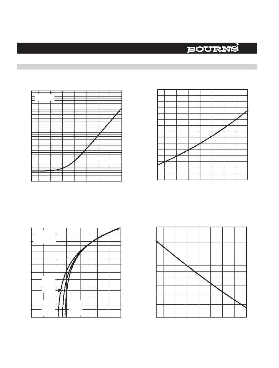
Typical Characteristics
TISP4xxxM3LM Overvoltage Protector Series
Figure 2.
Figure 3.
Figure 4.
Figure 5.
T
J
- Junction Temperature -
∞
C
-25
0
25
50
75
100
125
150
|I
D
|
-
Of
f-
S
t
ate Current -
µ
A
0∑001
0∑01
0∑1
1
10
100
TCMAG
V
D
=
±
50 V
T
J
- Junction Temperature -
∞
C
-25
0
25
50
75
100
125
150
Nor
m
a
l
i
ze
d
Br
e
akover
V
o
l
t
age
0.95
1.00
1.05
1.10
TC4MAF
V
T
- On-State Voltage - V
0.7
1.5
2
3
4
5
7
1
1
0
I
T
-
On-S
tate
Current - A
1.5
2
3
4
5
7
15
20
30
40
50
70
1
10
100
T
A
= 25
∞
C
t
W
= 100
µ
s
TC4MAJA
'4240
THRU
'4400
'4125
THRU
'4220
'4070
THRU
'4115
T
J
- Junction Temperature -
∞
C
-25
0
25
50
75
100
125
150
Nor
m
a
l
i
z
e
d
Ho
l
d
i
n
g
Current
0.4
0.5
0.6
0.7
0.8
0.9
1.5
2.0
1.0
TC4MAD
OFF-STATE CURRENT
vs
JUNCTION TEMPERATURE
NORMALIZED BREAKOVER VOLTAGE
vs
JUNCTION TEMPERATURE
ON-STATE CURRENT
vs
ON-STATE VOLTAGE
NORMALIZED HOLDING CURRENT
vs
JUNCTION TEMPERATURE

Specifications are subject to change without notice.
NOVEMBER 1997 - REVISED DECEMBER 2001
Typical Characteristics
Figure 6.
Figure 7.
V
D
- Off-state Voltage - V
0.5
1
2
3
5
10
20 30
50
100150
Cap
aci
t
a
nce No
rmal
i
zed to V
D
= 0
0.2
0.3
0.4
0.5
0.6
0.7
0.8
0.9
1
T
J
= 25
∞
C
V
d
= 1 Vrms
TC4MAKA
'4240 THRU '4400
'4125 THRU '4220
'4070 THRU '4115
V
DRM
- Repetitive Peak Off-State Voltage - V
50
60
70 80 90
150
200
250 300
100
C
-
Di
ff
erenti
al
O
f
f
-
S
t
at
e
Capaci
tance - pF
25
30
35
40
45
50
C = C
off(-2 V)
- C
off(-50 V)
TC4MALB
'
4070
'
4080
'
4095
'
4125
'
4145
'
4165
'
4180
'
4260
'
4300
'
4350
'
4400
'
4240
'
4115
'4220
'4250
'
4290
'
4395
NORMALIZED CAPACITANCE
vs
OFF-STATE VOLTAGE
DIFFERENTIAL OFF-STATE CAPACITANCE
vs
RATED REPETITIVE PEAK OFF-STATE VOLTAGE
TISP4xxxM3LM Overvoltage Protector Series

Specifications are subject to change without notice.
NOVEMBER 1997 - REVISED DECEMBER 2001
Rating and Thermal Information
TISP4xxxM3LM Overvoltage Protector Series
Figure 8.
Figure 9.
Figure 10.
Figure 11.
t - Current Duration - s
0∑1
1
10
100
1000
I
TS
M
(t)
-
N
on-
R
e
pet
i
t
i
ve P
eak O
n
-
S
t
a
t
e
C
u
r
r
ent
-
A
1.5
2
3
4
5
6
7
8
9
15
20
30
10
V
GEN
= 600 Vrms, 50/60 Hz
R
GEN
= 1.4*V
GEN
/I
TSM(t)
EIA/JESD51-2 ENVIRONMENT
EIA/JESD51-3 PCB
T
A
= 25
∞
C
t - Power Duration - s
0∑1
1
10
100
1000
Z
JA
(
t
)
- T
r
a
n
si
ent
Th
ermal
I
m
p
e
dance -
∞
C/W
4
5
6
7
8
9
15
20
30
40
50
60
70
80
90
150
10
100
TI4MAG
I
TSM(t)
APPLIED FOR TIME t
EIA/JESD51-2 ENVIRONMENT
EIA/JESD51-3 PCB
T
A
= 25
∞
C
T
AMIN
- Minimum Ambient Temperature -
∞
C
-35
-25
-15
-5
5
15
25
-40
-30
-20
-10
0
10
20
Derat
i
n
g
F
act
o
r
0.93
0.94
0.95
0.96
0.97
0.98
0.99
1.00
TI4MAHA
'4125 THRU '4220
'4240 THRU '4400
'4070 THRU '4115
T
A
- Ambient Temperature -
∞
C
-40 -30 -20 -10 0
10 20 30 40 50 60 70 80
Im
pulse C
u
rrent
-
A
40
50
60
70
80
90
100
120
150
200
250
300
400
IEC 1.2/50, 8/20
ITU-T 10/700
FCC 10/560
BELLCORE 2/10
BELLCORE 10/1000
FCC 10/160
TC4MAA
NON-REPETITIVE PEAK ON-STATE CURRENT
vs
CURRENT DURATION
THERMAL IMPEDANCE
vs
POWER DURATION
VDRM DERATING FACTOR
vs
MINIMUM AMBIENT TEMPERATURE
IMPULSE RATING
vs
AMBIENT TEMPERATURE

Specifications are subject to change without notice.
NOVEMBER 1997 - REVISED DECEMBER 2001
Deployment
TISP4xxxM3LM Overvoltage Protector Series
APPLICATIONS INFORMATION
These devices are two terminal overvoltage protectors. They may be used either singly to limit the voltage between two conductors (Figure 12)
or in multiples to limit the voltage at several points in a circuit (Figure 13).
In Figure 12, protector Th1 limits the maximum voltage between the two conductors to ±V(BO). This configuration is normally used to protect
circuits without a ground reference, such as modems. In Figure 13, protectors Th2 and Th3 limit the maximum voltage between each conduc-
tor and ground to the ±V(BO) of the individual protector. Protector Th1 limits the maximum voltage between the two conductors to its ±V(BO)
value. If the equipment being protected has all its vulnerable components connected between the conductors and ground, then protector Th1
is not required.
Impulse Testing
Standard
Peak Voltage
Setting
V
Voltage
Waveform
µs
Peak Current
Value
A
Current
Waveform
µs
TISP4xxxM3
25 ∞C Rating
A
Series
Resistance
GR-1089-CORE
2500
2/10
500
2/10
300
11
1000
10/1000
100
10/1000
50
FCC Part 68
(March 1998)
1500
10/160
200
10/160
120
2x5.6
800
10/560
100
10/560
75
3
1500
9/720
37.5
5/320
100
0
1000
9/720
25
5/320
100
0
I3124
1500
0.5/700
37.5
0.2/310
100
0
ITU-T K.20/K.21
1500
4000
10/700
37.5
100
5/310
100
0
FCC Part 68 terminology for the waveforms produced by the ITU-T recommendation K.21 10/700 impulse generator
To verify the withstand capability and safety of the equipment, standards require that the equipment is tested with various impulse wave forms.
The table below shows some common values
.
If the impulse generator current exceeds the protector's current rating, then a series resistance can be used to reduce the current to the
protector's rated value to prevent possible failure. The required value of series resistance for a given waveform is given by the following
calculations. First, the minimum total circuit impedance is found by dividing the impulse generator's peak voltage by the protector's rated
current. The impulse generator's fictive impedance (generator's peak voltage divided by peak short circuit current) is then subtracted from the
minimum total circuit impedance to give the required value of series resistance.
For the FCC Part 68 10/560 waveform the following values result. The minimum total circuit impedance is 800/75 = 10.7 and the generator's
fictive impedance is 800/100 = 8 . This gives a minimum series resistance value of 10.7 - 8 = 2.7 . After allowing for tolerance, a 3 ±10%
resistor would be suitable. The 10/160 waveform needs a standard resistor value of 5.6 per conductor. These would be R1a and R1b in
Figure 15 and Figure 16. FCC Part 68 allows the equipment to be non-operational after the 10/160 (conductor to ground) and 10/560 (inter-
conductor) impulses. The series resistor value may be reduced to zero to pass FCC Part 68 in a non-operational mode, e.g. Figure 14. For this
type of design, the series fuse must open before the TISP4xxxM3 fails. For Figure 14, the maximum fuse i
2
t is 2.3 A
2
s. In some cases, the
equipment will require verification over a temperature range. By using the rated waveform values from Figure 11, the appropriate series resistor
value can be calculated for ambient temperatures in the range of -40 ∞C to 85 ∞C.
Figure 12. Two Point Protection
Figure 13. Multi-point Protection
Th1
Th3
Th2
Th1

Specifications are subject to change without notice.
NOVEMBER 1997 - REVISED DECEMBER 2001
AC Power Testing
TISP4xxxM3LM Overvoltage Protector Series
Capacitance
Normal System Voltage Levels
JESD51 Thermal Measurement Method
APPLICATIONS INFORMATION
The protector can withstand currents applied for times not exceeding those shown in Figure 8. Currents that exceed these times must be
terminated or reduced to avoid protector failure. Fuses, PTC (Positive Temperature Coefficient) resistors and fusible resistors are overcurrent
protection devices which can be used to reduce the current flow. Protective fuses may range from a few hundred milliamperes to one ampere.
In some cases, it may be necessary to add some extra series resistance to prevent the fuse from opening during impulse testing. The current
versus time characteristic of the overcurrent protector must be below the line shown in Figure 8. In some cases there may be a further time
limit imposed by the test standard (e.g. UL 1459 wiring simulator failure).
The protector characteristic off-state capacitance values are given for d.c. bias voltage, VD, values of 0, -1 V, -2 V and -50 V. Where possible,
values are also given for -100 V. Values for other voltages may be calculated by multiplying the VD = 0 capacitance value by the factor given in
Figure 6. Up to 10 MHz, the capacitance is essentially independent of frequency. Above 10 MHz, the effective capacitance is strongly
dependent on connection inductance. In many applications, such as Figure 15 and Figure 17, the typical conductor bias voltages will be about
-2 V and -50 V. Figure 7 shows the differential (line unbalance) capacitance caused by biasing one protector at -2 V and the other at -50 V.
The protector should not clip or limit the voltages that occur in normal system operation. For unusual conditions, such as ringing without the
line connected, some degree of clipping is permissible. Under this condition, about 10 V of clipping is normally possible without activating the
ring trip circuit.
Figure 10 allows the calculation of the protector VDRM value at temperatures below 25 ∞C. The calculated value should not be less than the
maximum normal system voltages. The TISP4260M3LM, with a VDRM of 200 V, can be used for the protection of ring generators producing
100 V rms of ring on a battery voltage of -58 V (Th2 and Th3 in Figure 17). The peak ring voltage will be 58 + 1.414*100 = 199.4 V. However,
this is the open circuit voltage and the connection of the line and its equipment will reduce the peak voltage. In the extreme case of an
unconnected line, clipping the peak voltage to 190 V should not activate the ring trip. This level of clipping would occur at the temperature
when the VDRM has reduced to 190/200 = 0.95 of its 25 ∞C value. Figure 10 shows that this condition will occur at an ambient temperature of
-28 ∞C. In this example, the TISP4260M3LM will allow normal equipment operation provided that the minimum expected ambient temperature
does not fall below -28 ∞C.
To standardize thermal measurements, the EIA (Electronic Industries Alliance) has created the JESD51 standard. Part 2 of the standard
(JESD51-2, 1995) describes the test environment. This is a 0.0283 m3 (1 ft3) cube which contains the test PCB (Printed Circuit Board)
horizontally mounted at the center. Part 3 of the standard (JESD51-3, 1996) defines two test PCBs for surface mount components; one for
packages smaller than 27 mm (1.06 '') on a side and the other for packages up to 48 mm (1.89 ''). The LM package measurements used the
smaller 76.2 mm x 114.3 mm (3.0 '' x 4.5 '') PCB. The JESD51-3 PCBs are designed to have low effective thermal conductivity (high thermal
resistance) and represent a worse case condition. The PCBs used in the majority of applications will achieve lower values of thermal resistance
and so can dissipate higher power levels than indicated by the JESD51 values.

Specifications are subject to change without notice.
NOVEMBER 1997 - REVISED DECEMBER 2001
TISP4xxxM3LM Overvoltage Protector Series
Typical Circuits
Figure 14. MODEM Inter-wire Protection
Figure 15. Protection Module
Figure 16. ISDN Protection
Figure 17. Line Card Ring/Test Protection
FUSE
TISP4350
OR
TISP4400
AI6XBM
RING DETECTOR
HOOK SWITCH
D.C. SINK
SIGNAL
MODEM
RING
WIRE
TIP
WIRE
R1a
R1b
RING
WIRE
TIP
WIRE
Th3
Th2
Th1
PROTECTED
EQUIPMENT
E.G. L INE CARD
AI6XBK
R1a
R1b
Th3
Th2
Th1
AI6XBL
SIGNAL
D.C.
TEST
RELAY
RING
RELAY
SLIC
RELAY
TEST
EQUIP-
MENT
RING
GENERATOR
S1a
S1b
R1a
R1b
RING
WIRE
TIP
WIRE
Th3
Th2
Th1
Th4
Th5
SLIC
SLIC
PROTECTION
RING/TEST
PROTECTION
OVER-
CURRENT
PROTECTION
S2a
S2b
S3a
S3b
V
BAT
C1
220 nF
AI6XBJ
TISP6xxxx,
TISPPBLx,
1/2 TISP6NTP2

Specifications are subject to change without notice.
NOVEMBER 1997 - REVISED DECEMBER 2001
Device Symbolization Code
Device
Symbolization
Code
TISP4070M3LM
4070M3
TISP4080M3LM
4080M3
TISP4095M3LM
4095M3
TISP4115M3LM
4115M3
TISP4125M3LM
4125M3
TISP4145M3LM
4145M3
TISP4165M3LM
4165M3
TISP4180M3LM
4180M3
TISP4220M3LM
4220M3
TISP4240M3LM
4240M3
TISP4250M3LM
4250M3
TISP4260M3LM
4260M3
TISP4290M3LM
4290M3
TISP4300M3LM
4300M3
TISP4350M3LM
4350M3
TISP4395M3LM
4395M3
TISP4400M3LM
4400M3
MECHANICAL DATA
Carrier Information
Package Type
Carrier
Order #
Straight Lead DO-92
Bulk Pack
TISP4xxxM3LM
Straight Lead DO-92
Tape and Reeled
TISP4xxxM3LMR
Formed Lead DO-92
Tape and Reeled
TISP4xxxM3LMFR
TISP4xxxM3LM Overvoltage Protector Series
Devices will be coded as below.
Devices are shipped in one of the carriers below. A reel contains 2000 devices.

Specifications are subject to change without notice.
NOVEMBER 1997 - REVISED DECEMBER 2001
LM002 (DO-92) 2-Pin Cylindrical Plastic Package
MECHANICAL DATA
2-Pin Cylindrical Plastic Package
LM002 Package (DO-92)
MD4XARA
1
3
2
A
3
1
2
VIEW A
DIMENSIONS ARE:
METRIC
(INCHES)
4.44 - 5.21
(.175 - .205)
3.43
(.135)
4.32 - 5.34
(.170 - .210)
3.17 - 4.19
(.125 - .165)
2.03 - 2.67
(.080 - .105)
0.40 - 0.56
(.016 - .022)
0.35 - 0.41
(.014 - .016)
MIN.
2.20
(.086)
MAX.
12.7
(0.5)
MIN.
1.14 - 1.40
(.045 - .055)
2.41 - 2.67
(.095 - .105)
2.03 - 2.67
(.080 - .105)
This single-in-line package consists of a circuit mounted on a lead frame and encapsulated within a plastic compound. The compound will
withstand soldering temperature with no deformation, and circuit performance characteristics will remain stable when operated in high
humidity conditions. Leads require no additional cleaning or processing when used in soldered assembly.
TISP4xxxM3LM Overvoltage Protector Series

Specifications are subject to change without notice.
NOVEMBER 1997 - REVISED DECEMBER 2001
LM002 (DO-92) - Formed Leads Version- 2-Pin Cylindrical Plastic Package
MECHANICAL DATA
LMF002 (DO-92) - Formed Leads Version of LM002
MD4XASA
A
VIEW A
3
1
2
1
3
2
DIMRNSIONS ARE:
METRIC
(INCHES)
4.44 - 5.21
(.175 - .205)
3.43
(.135)
4.32 - 5.34
(.170 - .210)
3.17 - 4.19
(.125 - .165)
2.03 - 2.67
(.080 - .105)
2.03 - 2.67
(.080 - .105)
0.40 - 0.56
(.016 - .022)
0.35 - 0.41
(.014 - .016)
MIN.
2.20
(.086)
MAX.
4.00
(.157)
MAX.
2.40 - 2.90
(.094 - .114)
2.40 - 2.90
(.094 - .114)
This single-in-line package consists of a circuit mounted on a lead frame and encapsulated within a plastic compound. The compound will
withstand soldering temperature with no deformation, and circuit performance characteristics will remain stable when operated in high
humidity conditions. Leads require no additional cleaning or processing when used in soldered assembly.
TISP4xxxM3LM Overvoltage Protector Series

Specifications are subject to change without notice.
NOVEMBER 1997 - REVISED DECEMBER 2001
Tape Dimensions
MECHANICAL DATA
TISP4xxxM3LM Overvoltage Protector Series
LMF002 Package (Formed Lead DO-92) Tape
LMF002 Tape Dimensions Conform to
the Requirements of EIA-468-B
MD 4X A Q C
Adhesive Tape on Reverse
Side - Shown Dashed
Body Indent Visible
VIEW A
Tape Section
Shown in
View A
Flat of DO-92 Body
Towards Reel Axis
Direction of Feed
DIMENSIONS ARE:
METRIC
(INCHES)
4.88 - 5.28
(.192 - .208)
3.70 - 4.30
(.146 - .169)
23.00 - 32.00
(.906 - 1.260)
2.50
(.098)
3.41 - 4.21
(.134 - .166)
12.40 - 13.00
(.488 - .512)
11.70 - 13.70
(.461 - .539)
¯
MIN.
17.66 - 27.68
(.695 -1.090) 15.50 - 16.53
(.610 - .650)
8.50 - 11.00
(.335 - .433)
0.00 - 0.50
(0.00 - .020)
8.50 - 9.75
(.335 - .384)
5.50 - 19.00
(.217 - .748)
17.50 - 19.00
(.689 - .748)