TISP7070H3SL THRU TISP7095H3SL, TISP7125H3SL THRU TISP7210H3SL
TISP7250H3SL THRU TISP7400H3SL
TRIPLE BIDIRECTIONAL THYRISTOR OVERVOLTAGE PROTECTORS
P R O D U C T I N F O R M A T I O N
1
MARCH 1999 - REVISED MARCH 2000
Copyright © 2000, Power Innovations Limited, UK
Information is current as of publication date. Products conform to specifications in accordance
with the terms of Power Innovations standard warranty. Production processing does not
necessarily include testing of all parameters.
TELECOMMUNICATION SYSTEM 2x100 A 10/1000 OVERVOLTAGE PROTECTORS
G
Ion-Implanted Breakdown Region
- Precise DC and Dynamic Voltages
G
Rated for International Surge Wave Shapes
- Single and Simultaneous Impulses
DEVICE
V
DRM
V
V
(BO)
V
`7070
58
70
`7080
65
80
`7095
75
95
`7125
100
125
`7135
110
135
`7145
120
145
`7180
145
180
`7210
160
210
`7250
200
250
`7290
230
290
`7350
275
350
`7400
300
400
WAVE SHAPE
STANDARD
I
TSP
A
2/10 µs
GR-1089-CORE
500
8/20 µs
IEC 61000-4-5
350
10/160 µs
FCC Part 68
250
10/700 µs
FCC Part 68
ITU-T K20/21
200
10/560 µs
FCC Part 68
130
10/1000 µs
GR-1089-CORE
100
G
3-Pin Through-Hole Packaging
- Compatible with TO-220AB pin-out
- Low Height. . . . . . . . . . . . . . . . . . . . .8.3 mm
description
The TISP7xxxH3SL limits overvoltages between the telephone line Ring and Tip conductors and Ground.
Overvoltages are normally caused by a.c. power system or lightning flash disturbances which are induced or
conducted on to the telephone line.
Each terminal pair, T-G, R-G and T-R, has a symmetrical voltage-triggered bidirectional thyristor protection
characteristic. Overvoltages are initially clipped by breakdown clamping until the voltage rises to the
breakover level, which causes the device to crowbar into a low-voltage on state. This low-voltage on state
causes the current resulting from the overvoltage to be safely diverted through the device. The high crowbar
holding current prevents d.c. latchup as the diverted current subsides.
This TISP7xxxH3SL range consists of twelve voltage variants to meet various maximum system voltage
levels (58 V to 300 V). They are guaranteed to voltage limit and withstand the listed international lightning
surges in both polarities. These high current protection devices are in a 3-pin single-in-line (SL) plastic
package and are supplied in tube pack. For alternative impulse rating, voltage and holding current values in
SL packaged protectors, consult the factory. For lower rated impulse currents in the SL package, the 45 A
10/1000 TISP7xxxF3SL series is available.
These monolithic protection devices are fabricated in ion-implanted planar structures to ensure precise and
matched breakover control and are virtually transparent to the system in normal operation
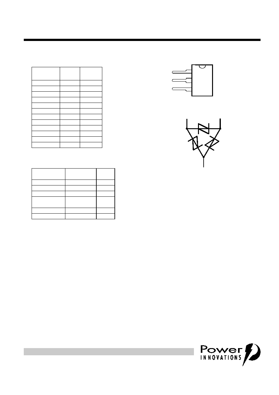
device symbol
G
T
R
SD7XAB
Terminals T, R and G correspond to the
alternative line designators of A, B and C
SL PACKAGE
(TOP VIEW)
1
2
3
T
G
R
MDXXAGA

TISP7070H3SL THRU TISP7095H3SL, TISP7125H3SL THRU TISP7210H3SL
TISP7250H3SL THRU TISP7400H3SL
TRIPLE BIDIRECTIONAL THYRISTOR OVERVOLTAGE PROTECTORS
2
MARCH 1999 - REVISED MARCH 2000
P R O D U C T I N F O R M A T I O N
absolute maximum ratings, T
A
= 25∞C (unless otherwise noted)
RATING
SYMBOL
VALUE
UNIT
Repetitive peak off-state voltage, (see Note 1)
`7070
`7080
`7095
`7125
`7135
`7145
`7180
`7210
`7250
`7290
`7350
`7400
V
DRM
± 58
± 65
± 75
±100
±110
±120
±145
±160
±200
±230
±275
±300
V
Non-repetitive peak on-state pulse current (see Notes 2, and 3)
I
TSP
A
2/10 (Telcordia GR-1089-CORE, 2/10 voltage wave shape)
500
8/20 µs (IEC 61000-4-5, 1.2/50 µs voltage, 8/20 current combination wave generator)
350
10/160 µs (FCC Part 68, 10/160 µs voltage wave shape)
250
4/250 (ITU-T K.20/21, 10/700 voltage wave shape, dual)
225
0.2/310 (CNET I 31-24, 0.5/700 voltage wave shape)
200
5/310 (ITU-T K.20/21, 10/700 voltage wave shape, single)
200
5/320 µs (FCC Part 68, 9/720 µs voltage wave shape)
200
10/560 µs (FCC Part 68, 10/560 µs voltage wave shape)
130
10/1000 (Telcordia GR-1089-CORE, 10/1000 voltage wave shape)
100
Non-repetitive peak on-state current (see Notes 2, 3 and 4)
I
TSM
55
60
0.9
A
20 ms (50 Hz) full sine wave
16.7 ms (60 Hz) full sine wave
1000 s 50 Hz/60 Hz a.c.
Initial rate of rise of on-state current,
Exponential current ramp, Maximum ramp value < 200 A
di
T
/dt
400
A/µs
Junction temperature
T
J
-40 to +150
∞C
Storage temperature range
T
stg
-65 to +150
∞C
NOTES: 1. Derate value at -0.13%/∞C for temperatures below 25 ∞C.
2. Initially the TISP7xxxH3 must be in thermal equilibrium.
3. These non-repetitive rated currents are peak values of either polarity. The rated current values may be applied to any terminal
pair. Additionally, both R and T terminals may have their rated current values applied simultaneously (in this case the G terminal
return current will be the sum of the currents applied to the R and T terminals). The surge may be repeated after the TISP7xxxH3
returns to its initial conditions.
4. EIA/JESD51-2 environment and EIA/JESD51-3 PCB with standard footprint dimensions connected with 5 A rated printed wiring
track widths. Derate current values at -0.61 %/∞C for ambient temperatures above 25 ∞C

3
MARCH 1999 - REVISED MARCH 2000
TISP7070H3SL THRU TISP7095H3SL, TISP7125H3SL THRU TISP7210H3SL
TISP7250H3SL THRU TISP7400H3SL
TRIPLE BIDIRECTIONAL THYRISTOR OVERVOLTAGE PROTECTORS
P R O D U C T I N F O R M A T I O N
electrical characteristics for any terminal pair, T
A
= 25∞C (unless otherwise noted)
PARAMETER
TEST CONDITIONS
MIN
TYP
MAX
UNIT
I
DRM
Repetitive peak off-
state current
V
D
= V
DRM
T
A
= 25∞C
T
A
= 85∞C
±5
±10
µA
V
(BO)
Breakover voltage
dv/dt = ±750 V/ms,
R
SOURCE
= 300
`7070
`7080
`7095
`7125
`7135
`7145
`7180
`7210
`7250
`7290
`7350
`7400
±70
±80
±95
±125
±135
±145
±180
±210
±250
±290
±350
±400
V
V
(BO)
Impulse breakover
voltage
dv/dt
±1000 V/µs, Linear voltage ramp,
Maximum ramp value = ±500 V
di/dt = ±20 A/µs, Linear current ramp,
Maximum ramp value = ±10 A
`7070
`7080
`7095
`7125
`7135
`7145
`7180
`7210
`7250
`7290
`7350
`7400
±78
±88
±103
±134
±144
±154
±189
±220
±261
±302
±362
±414
V
I
(BO)
Breakover current
dv/dt = ±750 V/ms,
R
SOURCE
= 300
±0.1
±0.8
A
V
T
On-state voltage
I
T
= ±5 A, t
W
= 100 µs
±5
V
I
H
Holding current
I
T
= ±5 A, di/dt = +/-30 mA/ms
±0.15
±0.6
A
dv/dt
Critical rate of rise of
off-state voltage
Linear voltage ramp, Maximum ramp value < 0.85V
DRM
±5
kV/µs
I
D
Off-state current
V
D
= ±50 V
T
A
= 85∞C
±10
µA
C
off
Off-state capacitance
f = 1 MHz,
V
d
= 1 V rms, V
D
= 0,
f = 1 MHz,
V
d
= 1 V rms, V
D
= -1 V
f = 1 MHz,
V
d
= 1 V rms, V
D
= -2 V
f = 1 MHz,
V
d
= 1 V rms, V
D
= -50 V
f = 1 MHz,
V
d
= 1 V rms, V
D
= -100 V
(see Note 5)
`7070 thru `7095
`7125 thru `7210
`7250 thru `7400
`7070 thru `7095
`7125 thru `7210
`7250 thru `7400
`7070 thru `7095
`7125 thru `7210
`7250 thru `7400
`7070 thru `7095
`7125 thru `7210
`7250 thru `7400
`7125 thru `7210
`7250 thru `7400
170
90
84
150
79
67
140
74
62
73
35
28
33
26
pF
NOTE
5: To avoid possible voltage clipping, the `7125 is tested with V
D
= -98 V.

TISP7070H3SL THRU TISP7095H3SL, TISP7125H3SL THRU TISP7210H3SL
TISP7250H3SL THRU TISP7400H3SL
TRIPLE BIDIRECTIONAL THYRISTOR OVERVOLTAGE PROTECTORS
4
MARCH 1999 - REVISED MARCH 2000
P R O D U C T I N F O R M A T I O N
thermal characteristics
PARAMETER
TEST CONDITIONS
MIN
TYP
MAX
UNIT
R
JA
Junction to free air thermal resistance
EIA/JESD51-3 PCB, I
T
= I
TSM(1000)
,
T
A
= 25 ∞C, (see Note 6)
50
∞C/W
NOTE
6:
EIA/JESD51-2 environment and PCB has standard footprint dimensions connected with 5 A rated printed wiring track widths.

5
MARCH 1999 - REVISED MARCH 2000
TISP7070H3SL THRU TISP7095H3SL, TISP7125H3SL THRU TISP7210H3SL
TISP7250H3SL THRU TISP7400H3SL
TRIPLE BIDIRECTIONAL THYRISTOR OVERVOLTAGE PROTECTORS
P R O D U C T I N F O R M A T I O N
PARAMETER MEASUREMENT INFORMATION
Figure 1. VOLTAGE-CURRENT CHARACTERISTIC FOR TERMINAL PAIRS
-v
V
DRM
I
DRM
V
D
I
H
I
T
V
T
I
TSM
I
TSP
V
(BO)
I
(BO)
I
D
Quadrant I
Switching
Characteristic
+v
+i
V
(BO)
I
(BO)
V
D
I
D
I
H
I
T
V
T
I
TSM
I
TSP
-i
Quadrant III
Switching
Characteristic
PM4XAAC
V
DRM
I
DRM
V
D
= ±50 V and I
D
= ±10 µA
used for reliability release