
TISP7125F3, TISP7150F3, TISP7180F3, TISP7240F3, TISP7260F3,
TISP7290F3, TISP7320F3, TISP7350F3, TISP7380F3
TRIPLE BIDIRECTIONAL THYRISTOR OVERVOLTAGE PROTECTORS
P R O D U C T I N F O R M A T I O N
1
MARCH 1994 - REVISED MARCH 2000
Copyright © 2000, Power Innovations Limited, UK
Information is current as of publication date. Products conform to specifications in accordance
with the terms of Power Innovations standard warranty. Production processing does not
necessarily include testing of all parameters.
TELECOMMUNICATION SYSTEM SECONDARY PROTECTION
G
Patented Ion-Implanted Breakdown Region
≠ Precise DC and Dynamic Voltages
G
Planar Passivated Junctions
≠ Low Off-State Current ....................< 10 µA
G
Rated for International Surge Wave Shapes
≠ Single and Simultaneous Impulses
G
..................UL Recognized Component
description
The TISP7xxxF3 series are 3-point overvoltage
protectors
designed
for
protecting
against
metallic (differential mode) and simultaneous
longitudinal
(common
mode)
surges.
Each
terminal pair has the same voltage limiting
values and surge current capability. This terminal
pair surge capability ensures that the protector
can meet the simultaneous longitudinal surge
requirement which is typically twice the metallic
surge requirement.
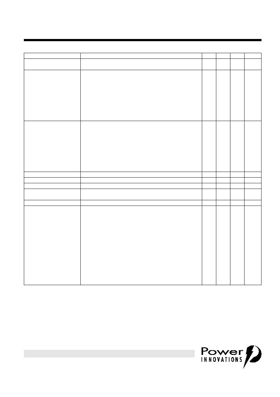
DEVICE
V
DRM
V
V
(BO)
V
`7125F3
100
125
`7150F3
120
150
`7180F3
145
180
`7240F3
180
240
`7260F3
200
260
`7290F3
220
290
`7320F3
240
320
`7350F3
275
350
`7380F3
270
380
For new designs use `7350F3 instead of `7380F3
WAVE SHAPE
STANDARD
I
TSP
A
2/10
GR-1089-CORE
190
8/20
IEC 61000-4-5
175
10/160
FCC Part 68
110
10/700
FCC Part 68
ITU-T K.20/21
70
10/560
FCC Part 68
50
10/1000
GR-1089-CORE
45
AVAILABLE OPTIONS
DEVICE
PACKAGE
CARRIER
ORDER #
TISP7xxxF3
D, Small-outline
TAPE AND REEL
TISP7xxxF3DR
TUBE
TISP7xxxF3D
TISP7xxxF3
P, Plastic DIP
TUBE
TISP7xxxF3P
TISP7xxxF3
SL, Single-in-line
TUBE
TISP7xxxF3SL
device symbol
G
T
R
SD7XAB
Terminals T, R and G correspond to the
alternative line designators of A, B and C
MD7XAACA
D PACKAGE
(TOP VIEW)
MDXXAL
G
NU
NU
G
NC
T
R
NC
1
2
3
4
5
6
7
8
MDXXAJA
1
2
3
4
5
6
7
8
R
NC
T
NC
G
NU
NU
G
P PACKAGE
(TOP VIEW)
NC - No internal connection
NU - Nonusable; no external electrical connection
should be made to these pins.
Specified ratings require connection of pin 5 and
pin 8.
SL PACKAGE
(TOP VIEW)
1
2
3
T
G
R
MDXXAGA

TISP7125F3, TISP7150F3, TISP7180F3, TISP7240F3, TISP7260F3,
TISP7290F3, TISP7320F3, TISP7350F3, TISP7380F3
TRIPLE BIDIRECTIONAL THYRISTOR OVERVOLTAGE PROTECTORS
2
MARCH 1994 - REVISED MARCH 2000
P R O D U C T I N F O R M A T I O N
description (continued)
Each terminal pair has a symmetrical voltage-triggered thyristor characteristic. Overvoltages are initially
clipped by breakdown clamping until the voltage rises to the breakover level, which causes the device to
crowbar into a low-voltage on state. This low-voltage on state causes the current resulting from the
overvoltage to be safely diverted through the device. The high crowbar holding current prevents d.c. latchup
as the diverted current subsides.These protectors are guaranteed to voltage limit and withstand the listed
lightning surges in both polarities.
These medium and high voltage devices are offered in nine voltage variants to meet a range battery and
ringing voltage requirements. They are guaranteed to suppress and withstand the listed international lightning
surges on any terminal pair. Similar devices with working voltages of 58 V and 66 V are detailed in the
TISP7072F3, TISP7082F3 data sheet.
absolute maximum ratings, T
A
= 25 ∞C (unless otherwise noted)
RATING
SYMBOL
VALUE
UNIT
Repetitive peak off-state voltage, 0 ∞C < T
A
< 70 ∞C
`7125F3
`7150F3
`7180F3
`7240F3
`7260F3
`7290F3
`7320F3
`7350F3
`7380F3
V
DRM
100
120
145
180
200
220
240
275
270
V
Non-repetitive peak on-state pulse current (see Notes 1 and 2)
I
PPSM
A
1/2 (Gas tube differential transient, 1/2 voltage wave shape)
330
2/10 (Telcordia GR-1089-CORE, 2/10 voltage wave shape)
190
1/20 (ITU-T K.22, 1.2/50 voltage wave shape, 25
resistor)
100
8/20 (IEC 61000-4-5, combination wave generator, 1.2/50 voltage wave shape)
175
10/160 (FCC Part 68, 10/160 voltage wave shape)
110
4/250 (ITU-T K.20/21, 10/700 voltage wave shape, simultaneous)
95
0.2/310 (CNET I 31-24, 0.5/700 voltage wave shape)
70
5/310 (ITU-T K.20/21, 10/700 voltage wave shape, single)
70
5/320 (FCC Part 68, 9/720 voltage wave shape, single)
70
10/560 (FCC Part 68, 10/560 voltage wave shape)
50
10/1000 (Telcordia GR-1089-CORE, 10/1000 voltage wave shape)
45
Non-repetitive peak on-state current, 0 ∞C < T
A
< 70 ∞C (see Notes 1 and 3)
50 Hz,
1 s
D Package
P Package
SL Package
I
TSM
4.3
5.7
7.1
A
Initial rate of rise of on-state current,
Linear current ramp, Maximum ramp value < 38 A
di
T
/dt
250
A/µs
Junction temperature
T
J
-65 to +150
∞C
Storage temperature range
T
stg
-65 to +150
∞C
NOTES: 1. Initially the TISP
Æ
must be in thermal equilibrium at the specified T
A
. The surge may be repeated after the TISP
Æ
returns to its
initial conditions. The rated current values may be applied singly either to the R to G or to the T to G or to the T to R terminals.
Additionally, both R to G and T to G may have their rated current values applied simultaneously (In this case the total G terminal
current will be twice the above rated current values).
2. See Thermal Information for derated I
PPSM
values 0 ∞C < T
A
< 70 ∞C and Applications Information for details on wave shapes.
3. Above 70 ∞C, derate I
TSM
linearly to zero at 150 ∞C lead temperature.
3
MARCH 1994 - REVISED MARCH 2000
TISP7125F3, TISP7150F3, TISP7180F3, TISP7240F3, TISP7260F3,
TISP7290F3, TISP7320F3, TISP7350F3, TISP7380F3
TRIPLE BIDIRECTIONAL THYRISTOR OVERVOLTAGE PROTECTORS
P R O D U C T I N F O R M A T I O N
electrical characteristics for all terminal pairs, T
A
= 25 ∞C (unless otherwise noted)
PARAMETER
TEST CONDITIONS
MIN
TYP
MAX
UNIT
I
DRM
Repetitive peak off-
state current
V
D
= V
DRM
, 0 ∞C < T
A
< 70 ∞C
±10
µA
V
(BO)
Breakover voltage
dv/dt = ±250 V/ms,
R
SOURCE
= 300
`7125F3
`7150F3
`7180F3
`7240F3
`7260F3
`7290F3
`7320F3
`7350F3
`7380F3
±125
±150
±180
±240
±260
±290
±320
±350
±380
V
V
(BO)
Impulse breakover
voltage
dv/dt
±1000 V/µs, Linear voltage ramp,
Maximum ramp value = ±500 V
di/dt = ±20 A/µs, Linear current ramp,
Maximum ramp value = ±10 A
`7125F3
`7150F3
`7180F3
`7240F3
`7260F3
`7290F3
`7320F3
`7350F3
`7380F3
±143
±168
±198
±269
±289
±319
±349
±379
±409
V
I
(BO)
Breakover current
dv/dt = ±250 V/ms,
R
SOURCE
= 300
±0.1
±0.8
A
V
T
On-state voltage
I
T
= ±5 A, t
W
= 100 µs
±5
V
I
H
Holding current
I
T
= ±5 A, di/dt = +/-30 mA/ms
±0.15
A
dv/dt
Critical rate of rise of
off-state voltage
Linear voltage ramp, Maximum ramp value < 0.85V
DRM
±5
kV/µs
I
D
Off-state current
V
D
= ±50 V
±10
µA
C
off
Off-state capacitance
f = 1 MHz,
V
d
= 1 V rms, V
D
= 0
f = 1 MHz,
V
d
= 1 V rms, V
D
= -1 V
f = 1 MHz,
V
d
= 1 V rms, V
D
= -2 V
f = 1 MHz,
V
d
= 1 V rms, V
D
= -5 V
f = 1 MHz,
V
d
= 1 V rms, V
D
= -50 V
f = 1 MHz,
V
d
= 1 V rms, V
D
= -100 V
f = 1 MHz,
V
d
= 1 V rms, V
DTR
= 0
(see Note 4)
`7125 thru `7180
`7240 thru `7380
`7125 thru `7180
`7240 thru `7380
`7125 thru `7180
`7240 thru `7380
`7125 thru `7180
`7240 thru `7380
`7125 thru `7180
`7240 thru `7380
`7125 thru `7180
`7240 thru `7380
`7125 thru `7180
`7240 thru `7380
37
31
40
34
36
30
31
24
17
13
14
10
20
17
48
41
52
44
47
39
40
31
23
17
18
13
27
23
pF
NOTE
4: Three-terminal guarded measurement, unmeasured terminal voltage bias is zero. First six capacitance values, with bias V
D
, are
for the R-G and T-G terminals only. The last capacitance value, with bias V
DTR
, is for the T-R terminals.

TISP7125F3, TISP7150F3, TISP7180F3, TISP7240F3, TISP7260F3,
TISP7290F3, TISP7320F3, TISP7350F3, TISP7380F3
TRIPLE BIDIRECTIONAL THYRISTOR OVERVOLTAGE PROTECTORS
4
MARCH 1994 - REVISED MARCH 2000
P R O D U C T I N F O R M A T I O N
thermal characteristics
PARAMETER
TEST CONDITIONS
MIN
TYP
MAX
UNIT
R
JA
Junction to free air thermal resistance
P
tot
= 0.8 W, T
A
= 25∞C
5 cm
2
, FR4 PCB
D Package
160
∞C/W
P Package
100
SL Package
135
PARAMETER MEASUREMENT INFORMATION
Figure 1. VOLTAGE-CURRENT CHARACTERISTIC FOR T AND R TERMINALS
T and G and R and G measurements are referenced to the G terminal
T and R measurements are referenced to the R terminal
-v
V
DRM
I
DRM
V
D
I
H
I
TSM
I
TSP
V
(BO)
I
(BO)
I
D
Quadrant I
Switching
Characteristic
+v
+i
V
(BO)
I
(BO)
V
DRM
I
DRM
V
D
I
D
I
H
I
TSM
I
TSP
-i
Quadrant III
Switching
Characteristic
PMXXAAA
5
MARCH 1994 - REVISED MARCH 2000
TISP7125F3, TISP7150F3, TISP7180F3, TISP7240F3, TISP7260F3,
TISP7290F3, TISP7320F3, TISP7350F3, TISP7380F3
TRIPLE BIDIRECTIONAL THYRISTOR OVERVOLTAGE PROTECTORS
P R O D U C T I N F O R M A T I O N
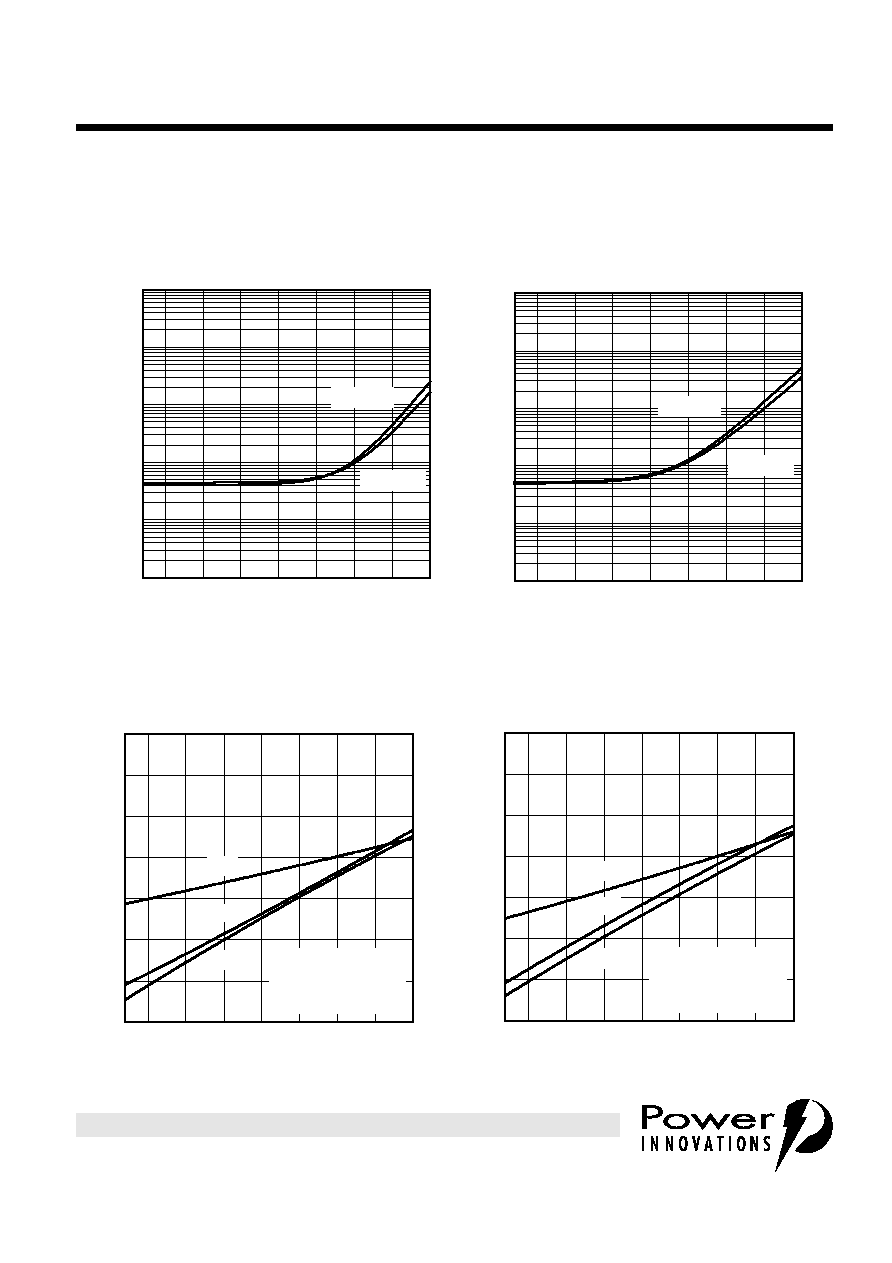
TYPICAL CHARACTERISTICS
R and G, or T and G terminals
TISP7125F3 THRU TISP7180F3
TISP7240F3 THRU TISP7380F3
Figure 2.
Figure 3.
Figure 4.
Figure 5.
OFF-STATE CURRENT
T
J
- Junction Temperature - ∞C
-25
0
25
50
75
100
125
150
I
D
-
O
ff-Sta
te
Cu
rre
n
t
-
µ
A
0∑001
0∑01
0∑1
1
10
100
TC7MAC
JUNCTION TEMPERATURE
vs
V
D
= -50 V
V
D
= 50 V
OFF-STATE CURRENT
T
J
- Junction Temperature - ∞C
-25
0
25
50
75
100
125
150
I
D
-
O
ff-S
ta
te
Cu
r
r
e
n
t
-
µ
A
0∑001
0∑01
0∑1
1
10
100
TC7HAC
JUNCTION TEMPERATURE
vs
V
D
= -50 V
V
D
= 50 V
NORMALISED BREAKDOWN VOLTAGES
T
J
- Junction Temperature - ∞C
-25
0
25
50
75
100
125
150
N
o
r
m
a
l
i
s
ed
B
r
eak
d
o
w
n
V
o
l
t
ag
es
0.9
1.0
1.1
1.2
TC7MAE
JUNCTION TEMPERATURE
vs
V
(BO)
V
(BR)
V
(BR)M
Positive Polarity
Normalised to V
(BR)
I
(BR)
= 1 mA and 25∞C
NORMALISED BREAKDOWN VOLTAGES
T
J
- Junction Temperature - ∞C
-25
0
25
50
75
100
125
150
N
o
r
m
a
lis
e
d
B
r
e
a
k
dow
n
V
ol
t
a
g
e
s
0.9
1.0
1.1
1.2
TC7HAE
JUNCTION TEMPERATURE
vs
V
(BO)
V
(BR)
V
(BR)M
Positive Polarity
Normalised to V
(BR)
I
(BR)
= 1 mA and 25∞C

TISP7125F3, TISP7150F3, TISP7180F3, TISP7240F3, TISP7260F3,
TISP7290F3, TISP7320F3, TISP7350F3, TISP7380F3
TRIPLE BIDIRECTIONAL THYRISTOR OVERVOLTAGE PROTECTORS
6
MARCH 1994 - REVISED MARCH 2000
P R O D U C T I N F O R M A T I O N
TYPICAL CHARACTERISTICS
R and G, or T and G terminals
TISP7125F3 THRU TISP7180F3
TISP7240F3 THRU TISP7380F3
Figure 6.
Figure 7.
Figure 8.
Figure 9.
NORMALISED BREAKDOWN VOLTAGES
T
J
- Junction Temperature - ∞C
-25
0
25
50
75
100
125
150
N
o
r
m
a
l
i
s
ed
B
r
eak
d
o
w
n
V
o
l
t
ag
es
0.9
1.0
1.1
1.2
TC7MAF
JUNCTION TEMPERATURE
vs
V
(BO)
V
(BR)
V
(BR)M
Negative Polarity
Normalised to V
(BR)
I
(BR)
= 1 mA and 25∞C
NORMALISED BREAKDOWN VOLTAGES
T
J
- Junction Temperature - ∞C
-25
0
25
50
75
100
125
150
N
o
r
m
al
i
s
ed
B
r
ea
kd
o
w
n
V
o
l
t
a
g
e
s
0.9
1.0
1.1
1.2
TC7HAF
JUNCTION TEMPERATURE
vs
V
(BO)
V
(BR)
V
(BR)M
Negative Polarity
Normalised to V
(BR)
I
(BR)
= 1 mA and 25∞C
ON-STATE CURRENT
V
T
- On-State Voltage - V
2
3
4
5
6
7 8 9
1
10
I
T
-
O
n-
S
t
a
t
e
C
u
r
r
e
nt
-
A
1
10
100
TC7MAL
ON-STATE VOLTAGE
vs
-40∞C
150∞C
25∞C
Positive Polarity
ON-STATE CURRENT
V
T
- On-State Voltage - V
2
3
4
5
6
7 8 9
1
10
I
T
-
O
n
-
S
t
a
t
e
C
u
rre
n
t
-
A
1
10
100
TC7HAL
ON-STATE VOLTAGE
vs
-40∞C
150∞C
25∞C
Positive Polarity

7
MARCH 1994 - REVISED MARCH 2000
TISP7125F3, TISP7150F3, TISP7180F3, TISP7240F3, TISP7260F3,
TISP7290F3, TISP7320F3, TISP7350F3, TISP7380F3
TRIPLE BIDIRECTIONAL THYRISTOR OVERVOLTAGE PROTECTORS
P R O D U C T I N F O R M A T I O N
TYPICAL CHARACTERISTICS
R and G, or T and G terminals
TISP7125F3 THRU TISP7180F3
TISP7240F3 THRU TISP7380F3
Figure 10.
Figure 11.
Figure 12.
Figure 13.
ON-STATE CURRENT
V
T
- On-State Voltage - V
2
3
4
5
6
7 8 9
1
10
I
T
-
O
n-
S
t
a
t
e
C
u
r
r
e
nt
-
A
1
10
100
TC7MAM
ON-STATE VOLTAGE
vs
-40∞C
150∞C
25∞C
Negative Polarity
ON-STATE CURRENT
V
T
- On-State Voltage - V
2
3
4
5
6
7 8 9
1
10
I
T
-
O
n-
S
t
a
t
e
C
ur
r
e
nt
-
A
1
10
100
TC7HAM
ON-STATE VOLTAGE
vs
-40∞C
150∞C
25∞C
Negative Polarity
HOLDING CURRENT & BREAKOVER CURRENT
T
J
- Junction Temperature - ∞C
-25
0
25
50
75
100
125
150
I
H
,I
(BO
)
-
H
o
l
di
ng
C
u
r
r
e
nt
,
B
r
e
a
k
o
v
e
r
C
u
r
r
e
n
t
-
A
0.2
0.3
0.4
0.5
0.6
0.7
0.8
0.9
0.1
1.0
HOLDING CURRENT & BREAKOVER CURRENT
T
J
- Junction Temperature - ∞C
-25
0
25
50
75
100
125
150
I
H
,I
(BO
)
-
H
o
l
d
i
n
g
Cu
rre
n
t
,
B
re
a
k
o
v
e
r
Cu
rre
n
t
-
A
0∑06
0∑07
0∑08
0∑09
0∑2
0∑3
0∑4
0∑5
0∑6
0∑7
0∑8
0∑9
0∑1
1∑0
TC7HAH
JUNCTION TEMPERATURE
vs
I
H
+I
(BO)
-I
(BO)

TISP7125F3, TISP7150F3, TISP7180F3, TISP7240F3, TISP7260F3,
TISP7290F3, TISP7320F3, TISP7350F3, TISP7380F3
TRIPLE BIDIRECTIONAL THYRISTOR OVERVOLTAGE PROTECTORS
8
MARCH 1994 - REVISED MARCH 2000
P R O D U C T I N F O R M A T I O N
TYPICAL CHARACTERISTICS
R and G, or T and G terminals
TISP7125F3 THRU TISP7180F3
TISP7240F3 THRU TISP7380F3
Figure 14.
Figure 15.
Figure 16.
Figure 17.
NORMALISED BREAKOVER VOLTAGE
di/dt - Rate of Rise of Principle Current - A/µs
0∑001
0∑01
0∑1
1
10
100
N
o
r
m
al
i
s
ed
B
r
ea
k
o
ve
r
V
o
l
t
a
g
e
1.0
1.1
1.2
TC7MAU
Positive
RATE OF RISE OF PRINCIPLE CURRENT
vs
Negative
NORMALISED BREAKOVER VOLTAGE
di/dt - Rate of Rise of Principle Current - A/µs
0∑001
0∑01
0∑1
1
10
100
N
o
r
m
al
i
s
ed
B
r
ea
k
o
ve
r
V
o
l
t
a
g
e
1.0
1.1
1.2
TC7HAU
Positive
RATE OF RISE OF PRINCIPLE CURRENT
vs
Negative
SURGE CURRENT
Decay Time - µs
10
100
1000
M
a
x
i
m
u
m
S
u
r
ge
C
u
r
r
e
nt
-
A
10
100
1000
TC7MAA
vs
DECAY TIME
2
SURGE CURRENT
Decay Time - µs
10
100
1000
M
a
x
i
m
u
m
S
u
r
ge
C
u
r
r
e
nt
-
A
10
100
1000
TC7HAA
vs
DECAY TIME
2

9
MARCH 1994 - REVISED MARCH 2000
TISP7125F3, TISP7150F3, TISP7180F3, TISP7240F3, TISP7260F3,
TISP7290F3, TISP7320F3, TISP7350F3, TISP7380F3
TRIPLE BIDIRECTIONAL THYRISTOR OVERVOLTAGE PROTECTORS
P R O D U C T I N F O R M A T I O N
TYPICAL CHARACTERISTICS
R and T terminals
TISP7125F3 THRU TISP7180F3
TISP7240F3 THRU TISP7380F3
Figure 18.
Figure 19.
Figure 20.
Figure 21.
OFF-STATE CURRENT
T
J
- Junction Temperature - ∞C
-25
0
25
50
75
100
125
150
I
D
-
O
ff
-Sta
te
Cu
rre
n
t
-
µ
A
0∑001
0∑01
0∑1
1
10
100
TC7MAD
JUNCTION TEMPERATURE
vs
OFF-STATE CURRENT
T
J
- Junction Temperature - ∞C
-25
0
25
50
75
100
125
150
I
D
-
O
ff
-Sta
te
Cu
rre
n
t
-
µ
A
0∑001
0∑01
0∑1
1
10
100
TC7HAD
JUNCTION TEMPERATURE
vs
NORMALISED BREAKDOWN VOLTAGES
T
J
- Junction Temperature - ∞C
-25
0
25
50
75
100
125
150
N
o
r
m
a
lis
e
d
B
r
e
a
k
dow
n
V
ol
t
a
g
e
s
0.9
1.0
1.1
1.2
TC7MAG
JUNCTION TEMPERATURE
vs
V
(BO)
V
(BR)
V
(BR)M
NORMALISED BREAKDOWN VOLTAGES
T
J
- Junction Temperature - ∞C
-25
0
25
50
75
100
125
150
N
o
r
m
a
l
i
s
ed
B
r
eak
do
w
n
V
o
l
t
ag
es
0.9
1.0
1.1
1.2
TC7HAG
JUNCTION TEMPERATURE
vs
V
(BO)
V
(BR)
V
(BR)M

TISP7125F3, TISP7150F3, TISP7180F3, TISP7240F3, TISP7260F3,
TISP7290F3, TISP7320F3, TISP7350F3, TISP7380F3
TRIPLE BIDIRECTIONAL THYRISTOR OVERVOLTAGE PROTECTORS
10
MARCH 1994 - REVISED MARCH 2000
P R O D U C T I N F O R M A T I O N
TYPICAL CHARACTERISTICS
R and T terminals
TISP7125F3 THRU TISP7180F3
TISP7240F3 THRU TISP7380F3
Figure 22.
Figure 23.
Figure 24.
Figure 25.
ON-STATE CURRENT
V
T
- On-State Voltage - V
2
3
4
5
6
7 8 9
1
10
I
T
-
O
n-
St
at
e
C
u
r
r
e
nt
-
A
1
10
100
TC7MAK
ON-STATE VOLTAGE
vs
-40∞C
150∞C
25∞C
ON-STATE CURRENT
V
T
- On-State Voltage - V
2
3
4
5
6
7 8 9
1
10
I
T
-
O
n-
St
at
e
C
u
r
r
e
nt
-
A
1
10
100
TC7HAK
ON-STATE VOLTAGE
vs
-40∞C
150∞C
25∞C
HOLDING CURRENT & BREAKOVER CURRENT
T
J
- Junction Temperature - ∞C
-25
0
25
50
75
100
125
150
I
H
,I
(BO
)
-
H
o
l
di
ng
C
u
r
r
e
nt
,
B
r
e
a
k
o
v
er
C
u
r
r
e
n
t
-
A
0.2
0.3
0.4
0.5
0.6
0.7
0.8
0.9
0.1
1.0
TC7MAJ
JUNCTION TEMPERATURE
vs
I
H
I
(BO)
HOLDING CURRENT & BREAKOVER CURRENT
T
J
- Junction Temperature - ∞C
-25
0
25
50
75
100
125
150
I
H
,I
(BO
)
-
H
o
l
d
i
n
g
Cu
rre
n
t
,
B
re
a
k
o
v
e
r
Cu
rre
n
t
-
A
0∑06
0∑07
0∑08
0∑09
0∑2
0∑3
0∑4
0∑5
0∑6
0∑7
0∑8
0∑9
0∑1
1∑0
TC7HAJ
JUNCTION TEMPERATURE
vs
I
H
I
(BO)

11
MARCH 1994 - REVISED MARCH 2000
TISP7125F3, TISP7150F3, TISP7180F3, TISP7240F3, TISP7260F3,
TISP7290F3, TISP7320F3, TISP7350F3, TISP7380F3
TRIPLE BIDIRECTIONAL THYRISTOR OVERVOLTAGE PROTECTORS
P R O D U C T I N F O R M A T I O N
TYPICAL CHARACTERISTICS
R and T terminals
TISP7125F3 THRU TISP7180F3
TISP7240F3 THRU TISP7380F3
Figure 26.
Figure 27.
NORMALISED BREAKOVER VOLTAGE
di/dt - Rate of Rise of Principle Current - A/µs
0∑001
0∑01
0∑1
1
10
100
No
rm
a
l
i
s
e
d
Bre
a
k
o
v
e
r
V
o
l
ta
g
e
1.0
1.1
1.2
TC7MAV
RATE OF RISE OF PRINCIPLE CURRENT
vs
NORMALISED BREAKOVER VOLTAGE
di/dt - Rate of Rise of Principle Current - A/µs
0∑001
0∑01
0∑1
1
10
100
No
rm
a
l
i
s
e
d
Bre
a
k
o
v
e
r
V
o
l
ta
g
e
1.0
1.1
1.2
TC7HAV
RATE OF RISE OF PRINCIPLE CURRENT
vs

TISP7125F3, TISP7150F3, TISP7180F3, TISP7240F3, TISP7260F3,
TISP7290F3, TISP7320F3, TISP7350F3, TISP7380F3
TRIPLE BIDIRECTIONAL THYRISTOR OVERVOLTAGE PROTECTORS
12
MARCH 1994 - REVISED MARCH 2000
P R O D U C T I N F O R M A T I O N
THERMAL INFORMATION
TISP7125F3 THRU TISP7180F3
TISP7240F3 THRU TISP7380F3
Figure 28.
Figure 29.
Figure 30.
Figure 31.
MAXIMUM NON-RECURRING 50 Hz CURRENT
t - Current Duration - s
0∑1
1
10
100
1000
I
TR
M
S
-
M
a
x
i
m
u
m
No
n
-
Re
c
u
rre
n
t
5
0
Hz
Cu
rre
n
t
-
A
1
10
vs
CURRENT DURATION
TI7MAA
V
GEN
= 250 Vrms
R
GEN
= 10 to 150
D Package
SL Package
P Package
MAXIMUM NON-RECURRING 50 Hz CURRENT
t - Current Duration - s
0∑1
1
10
100
1000
I
TR
M
S
-
M
a
x
i
m
u
m
No
n
-
Re
c
u
rre
n
t
5
0
Hz
Cu
rre
n
t
-
A
1
10
vs
CURRENT DURATION
TI7HAA
D Package
SL Package
P Package
V
GEN
= 350 Vrms
R
GEN
= 20 to 250
THERMAL RESPONSE
t - Power Pulse Duration - s
0∑0001 0∑001
0∑01
0∑1
1
10
100
1000
Z
J
-
T
r
a
n
s
i
e
n
t
The
r
m
al
Im
pe
da
nc
e
-
∞
C
/W
1
10
100
D Package
P Package
TI7MAB
SL Package
THERMAL RESPONSE
t - Power Pulse Duration - s
0∑0001 0∑001
0∑01
0∑1
1
10
100
1000
Z
J
-
T
r
a
n
s
i
e
n
t
The
r
m
al
Im
pe
da
nc
e
-
∞
C
/W
1
10
100
D Package
P Package
TI7MAB
SL Package

13
MARCH 1994 - REVISED MARCH 2000
TISP7125F3, TISP7150F3, TISP7180F3, TISP7240F3, TISP7260F3,
TISP7290F3, TISP7320F3, TISP7350F3, TISP7380F3
TRIPLE BIDIRECTIONAL THYRISTOR OVERVOLTAGE PROTECTORS
P R O D U C T I N F O R M A T I O N
THERMAL INFORMATION
Non-repetitive peak on-state pulse derated values for 0 ∞C
T
A
70 ∞C
RATING
SYMBOL
VALUE
UNIT
Non-repetitive peak on-state pulse current, 0 ∞C < T
A
< 70 ∞C (see Notes 5, 6 and 7)
I
PPSM
A
1/2 (Gas tube differential transient, 1/2 voltage wave shape)
320
2/10 (Telcordia GR-1089-CORE, 2/10 voltage wave shape)
175
1/20 (ITU-T K.22, 1.2/50 voltage wave shape, 25
resistor)
90
8/20 (IEC 61000-4-5, combination wave generator, 1.2/50 voltage wave shape)
150
10/160 (FCC Part 68, 10/160 voltage wave shape)
90
4/250 (ITU-T K.20/21, 10/700 voltage wave shape, dual)
70
0.2/310 (CNET I 31-24, 0.5/700 voltage wave shape)
65
5/310 (ITU-T K.20/21, 10/700 voltage wave shape, single)
65
5/320 (FCC Part 68, 9/720 voltage wave shape)
65
10/560 (FCC Part 68, 10/560 voltage wave shape)
45
10/1000 (Telcordia GR-1089-CORE, 10/1000 voltage wave shape)
40
NOTES: 5. Initially the TISP
Æ
must be in thermal equilibrium at the specified T
A
. The impulse may be repeated after the TISP
Æ
returns to its
initial conditions. The rated current values may be applied either to the R to G or to the T to G or to the T to R terminals.
Additionally, both R to G and T to G may have their rated current values applied simultaneously (In this case the total G terminal
current will be twice the above rated current values).
6. See Applications Information for details on wave shapes.
7. Above 70 ∞C, derate I
PPSM
linearly to zero at 150 ∞C lead temperature.

TISP7125F3, TISP7150F3, TISP7180F3, TISP7240F3, TISP7260F3,
TISP7290F3, TISP7320F3, TISP7350F3, TISP7380F3
TRIPLE BIDIRECTIONAL THYRISTOR OVERVOLTAGE PROTECTORS
14
MARCH 1994 - REVISED MARCH 2000
P R O D U C T I N F O R M A T I O N
APPLICATIONS INFORMATION
deployment
These devices are three terminal overvoltage protectors. They limit the voltage between three points in the
circuit. Typically, this would be the two line conductors and protective ground (Figure 32).
In Figure 32, protectors Th2 and Th3 limit the maximum voltage between each conductor and ground to the
±V
(BO)
of the individual protector. Protector Th1 limits the maximum voltage between the two conductors to its
±V
(BO)
value.
lightning surge
wave shape notation
Most lightning tests, used for equipment verification, specify a unidirectional sawtooth waveform which has an
exponential rise and an exponential decay. Wave shapes are classified in terms of rise time in microseconds
and a decay time in microseconds to 50% of the maximum amplitude. The notation used for the wave shape
is
rise time/decay time
, without the microseconds quantity and the "/" between the two values has no
mathematical significance. A 50A, 5/310 waveform would have a peak current value of 50 A, a rise time of
5 µs and a decay time of 310 µs. The TISP
Æ
surge current graph comprehends the wave shapes of commonly
used surges.
generators
There are three categories of surge generator type: single wave shape, combination wave shape and circuit
defined. Single wave shape generators have essentially the same wave shape for the open circuit voltage and
short circuit current (e.g. 10/1000 open circuit voltage and short circuit current). Combination generators have
two wave shapes, one for the open circuit voltage and the other for the short circuit current (e.g. 1.2/50 open
circuit voltage and 8/20 short circuit current) Circuit specified generators usually equate to a combination
generator, although typically only the open circuit voltage wave shape is referenced (e.g. a 10/700 open
circuit voltage generator typically produces a 5/310 short circuit current). If the combination or circuit defined
generators operate into a finite resistance the wave shape produced is intermediate between the open circuit
and short circuit values.
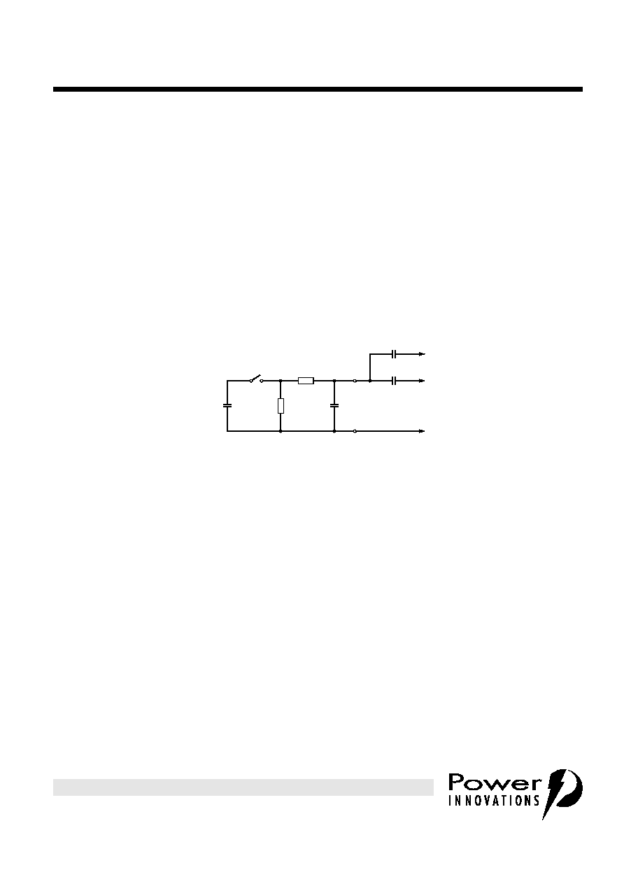
ITU-T 10/700 generator
This circuit defined generator is specified in many standards. The descriptions and values are not consistent
between standards and it is important to realise that it is always the same generator being used.
Figure 33 shows the 10/700 generator circuit defined in ITU-T recommendation K.20 (10/96) "Resistibility of
telecommunication switching equipment to overvoltages and overcurrents". The basic generator comprises
of:
capacitor C
1
, charged to voltage V
C
, which is the energy storage element.
switch SW to discharge the capacitor into the output shaping network
Figure 32. MULTI-POINT PROTECTION
Th3
Th2
Th1

15
MARCH 1994 - REVISED MARCH 2000
TISP7125F3, TISP7150F3, TISP7180F3, TISP7240F3, TISP7260F3,
TISP7290F3, TISP7320F3, TISP7350F3, TISP7380F3
TRIPLE BIDIRECTIONAL THYRISTOR OVERVOLTAGE PROTECTORS
P R O D U C T I N F O R M A T I O N
shunt resistor R
1
, series resistor R
2
and shunt capacitor C
2
form the output shaping network.
series feed resistor R
3
to connect to one line conductor for single surge
series feed resistor R
4
to connect to the other line conductor for dual surging
In the normal single surge equipment test configuration, the unsurged line is grounded. This is shown by the
dotted lines in the top drawing of Figure 33. However, doing this at device test places one terminal pair in
parallel with another terminal pair. To check the individual terminal pairs of the TISP7xxxF3, without any
paralleled operation, the unsurged terminal is left unconnected.
With the generator output open circuit, when SW closes, C1 discharges through R
1
. The decay time constant
will be C
1
R
1
, or 20 x 50 = 1000 µs. For the 50% voltage decay time the time constant needs to be multiplied
by 0.697, giving 0.697 x 1000 = 697 µs which is rounded to 700 µs.
The output rise time is controlled by the time constant of R
2
and C
2
. which is 15 x 200 = 3000 ns or 3 µs.
Virtual voltage rise times are given by straight line extrapolation through the 30% and 90% points of the
voltage waveform to zero and 100%. Mathematically this is equivalent to 3.24 times the time constant, which
gives 3.24 x 3 = 9.73 which is rounded to 10 µs. Thus the open circuit voltage rises in 10 µs and decays in
700 µs, giving the 10/700 generator its name.
When the overvoltage protector switches it effectively shorts the generator output via the series 25
resistor.
Two short circuit conditions need to be considered: single output using R
3
only (top circuit of Figure 33) and
dual output using R
3
and R
4
(bottom circuit of Figure 33).
For the single test, the series combination of R
2
and R
3
(15 + 25 = 40
) is in shunt with R
1
. This lowers the
discharge resistance from 50
to 22.2
, giving a discharge time constant of 444 µs and a 50% current
decay time of 309.7 µs, which is rounded to 310 µs.
For the rise time, R
2
and R
3
are in parallel, reducing the effective source resistance from 15
to 9.38
,
giving a time constant of 1.88 µs. Virtual current rise times are given by straight line extrapolation through the
10% and 90% points of the current waveform to zero and 100%. Mathematically this is equivalent to 2.75
Figure 33.
C
2
200 nF
R
1
50
C
1
20 µF
R
2
15
SW
V
C
2.8 kV
R
3
25
R
T
T
G
T
R
G
R
G
T AND G
TEST
R AND G
TEST
R AND T
TEST
70 A
5/310
70 A
5/310
10/700 GENERATOR - SINGLE TERMINAL PAIR TEST
C
2
200 nF
R
1
50
C
1
20 µF
R
2
15
SW
R
3
25
R
4
25
R
T
G
DUAL
T AND G,
R AND G
TEST
95 A
4/250
95 A
4/250
190 A
4/250
V
C
5.2 kV
10/700 GENERATOR - DUAL TERMINAL PAIR TEST

TISP7125F3, TISP7150F3, TISP7180F3, TISP7240F3, TISP7260F3,
TISP7290F3, TISP7320F3, TISP7350F3, TISP7380F3
TRIPLE BIDIRECTIONAL THYRISTOR OVERVOLTAGE PROTECTORS
16
MARCH 1994 - REVISED MARCH 2000
P R O D U C T I N F O R M A T I O N
times the time constant, which gives 2.75 x 1.88 = 5.15, which is rounded to 5 µs. Thus the short circuit
current rises in 5 µs and decays in 310 µs, giving the 5/310 wave shape.
The series resistance from C
1
to the output is 40
giving an output conductance of 25 A/kV. For each 1 kV of
capacitor charge voltage, 25 A of output current will result.
For the dual test, the series combination of R
2
plus R
3
and R
4
in parallel (15 + 12.5 = 27.5
) is in shunt with
R
1
. This lowers the discharge resistance from 50
to 17.7
, giving a discharge time constant of 355 µs and
a 50% current decay time of 247 µs, which is rounded to 250 µs.
For the rise time, R
2
, R
3
and R
4
are in parallel, reducing the effective source resistance from 15
to 6.82
,
giving a time constant of 1.36 µs, which gives a current rise time of 2.75 x 1.36 = 3.75, which is rounded to
4 µs. Thus the short circuit current rises in 4 µs and decays in 250 µs, giving the 4/250 wave shape.
The series resistance from C
1
to an
individual
output is 2 x 27.5 = 55
giving an output conductance of
18 A/kV. For each 1 kV of capacitor charge voltage, 18 A of output current will result.
At 25 ∞C these protectors are rated at 70 A for the single terminal pair condition and 95 A for the dual
condition (R and G terminals and T and G terminals). In terms of generator voltage, this gives a maximum
generator setting of 70 x 40 = 2.8 kV for the single condition and 2 x 95 x 27.5 = 5.2 kV for the dual condition.
The higher generator voltage setting for the dual condition is due to the current waveform decay being shorter
at 250 µs compared to the 310 µs value of the single condition.
Other ITU-T recommendations use the 10/700 generator: K.17 (11/88) "Tests on power-fed repeaters using
solid-state devices in order to check the arrangements for protection from external interference" and K.21(10/
96) "Resistibility of subscriber's terminal to overvoltages and overcurrents", K.30 (03/93) "Positive
temperature coefficient (PTC) thermistors".
Several IEC publications use the 10/700 generator, common ones are IEC 6100-4-5 (03/95) "Electromagnetic
compatibility (EMC) - Part 4: Testing and measurement techniques - Section 5: Surge immunity test" and IEC
60950 (04/99) "Safety of information technology equipment".
The IEC 60950 10/700 generator is carried through into other "950" derivatives. Europe is harmonised by
CENELEC (ComitÈ EuropÈen de Normalization Electro-technique) under EN 60950 (included in the Low
Voltage Directive, CE mark). US has UL (Underwriters Laboratories) 1950 and Canada CSA (Canadian
Standards Authority) C22.2 No. 950.
FCC Part 68 "Connection of terminal equipment to the telephone network" (47 CFR 68) uses the 10/700
generator for Type B surge testing. Part 68 defines the open circuit voltage wave shape as 9/720 and the
short circuit current wave shape as 5/320 for a single output. The current wave shape in the dual (longitudinal)
test condition is not defined, but it can be assumed to be 4/250.
Several VDE publications use the 10/700 generator, for example: VDE 0878 Part 200 (12/92)
"Electromagnetic compatibility of information technology equipment and telecommunications equipment;
Immunity of analogue subscriber equipment".
1.2/50 generators
The 1.2/50 open circuit voltage and 8/20 short circuit current combination generator is defined in IEC 61000-
4-5 (03/95) "Electromagnetic compatibility (EMC) - Part 4: Testing and measurement techniques - Section 5:
Surge immunity test". This generator has a fictive output resistance of 2
, meaning that dividing the open
circuit output voltage by the short circuit output current gives a value of 2
(500 A/kV).
17
MARCH 1994 - REVISED MARCH 2000
TISP7125F3, TISP7150F3, TISP7180F3, TISP7240F3, TISP7260F3,
TISP7290F3, TISP7320F3, TISP7350F3, TISP7380F3
TRIPLE BIDIRECTIONAL THYRISTOR OVERVOLTAGE PROTECTORS
P R O D U C T I N F O R M A T I O N
The combination generator has three testing configurations; directly applied for testing between equipment
a.c. supply connections, applied via an external 10
resistor for testing between the a.c. supply connections
and ground, and applied via an external 40
resistor for testing all other lines. For unshielded unsymmetrical
data or signalling lines, the combination generator is applied via a 40
resistor either between lines or line to
ground. For unshielded symmetrical telecommunication lines, the combination generator is applied to all lines
via a resistor of n x 40
, where n is the number of conductors and the maximum value of external feed
resistance is 250
. Thus for four conductors n = 4 and the series resistance is 4 x 40 = 160
. For ten
conductors the resistance cannot be 10 x 40 = 400
and must be 250
. The combination generator is used
for short distance lines, long distance lines are tested with the 10/700 generator.
When the combination generator is used with a 40
, or more, external resistor, the current wave shape is not
8/20, but becomes closer to the open circuit voltage wave shape of 1.2/50. For example, a commercial
generator when used with 40
produced an 1.4/50 wave shape.
The wave shapes of 1.2/50 and 8/20 occur in other generators as well. British Telecommunication has a
combination generator with 1.2/50 voltage and 8/20 current wave shapes, but it has a fictive resistance of 1
.
ITU-T recommendation K.22 "Overvoltage resistibility of equipment connected to an ISDN T/S BUS" (05/95)
has a 1.2/50 generator option using only resistive and capacitive elements, Figure 34.
The K.22 generator produces a 1.4/53 open circuit voltage wave. Using 25
output resistors, gives a single
short circuit current output wave shape of 0.8/18 with 26 A/kV and a dual of 0.6/13 with 20 A/kV. These
current wave shapes are often rounded to 1/20 and 0.8/14.
There are 8/20 short circuit current defined generators. These are usually very high current, 10 kA or more
and are used for testing a.c. protectors, primary protection modules and some Gas Discharge Tubes.
impulse testing
To verify the withstand capability and safety of the equipment, standards require that the equipment is tested
with various impulse wave forms. The table in this section shows some common test values.
Manufacturers are being increasingly required to design in protection coordination. This means that each
protector is operated at its design level and currents are diverted through the appropriate protector e.g. the
primary level current through the primary protector and lower levels of current may be diverted through the
secondary or inherent equipment protection. Without coordination, primary level currents could pass through
the equipment only designed to pass secondary level currents. To ensure coordination happens with fixed
voltage protectors, some resistance is normally used between the primary and secondary protection (R1a
and R1b Figure 36). The values given in this data sheet apply to a 400 V (d.c. sparkover) gas discharge tube
primary protector and the appropriate test voltage when the equipment is tested with a primary protector.
Figure 34.
C
2
30 nF
R
1
76
C
1
1 µF
R
2
13
SW
V
C
1 kV
K.22 1.2/50 GENERATOR
C
3
8 nF
C
4
8 nF
NOTE: SOME STANDARDS
REPLACE OUTPUT
CAPACITORS WITH
25
RESISTORS

TISP7125F3, TISP7150F3, TISP7180F3, TISP7240F3, TISP7260F3,
TISP7290F3, TISP7320F3, TISP7350F3, TISP7380F3
TRIPLE BIDIRECTIONAL THYRISTOR OVERVOLTAGE PROTECTORS
18
MARCH 1994 - REVISED MARCH 2000
P R O D U C T I N F O R M A T I O N
If the impulse generator current exceeds the protectors current rating then a series resistance can be used to
reduce the current to the protectors rated value and so prevent possible failure. The required value of series
resistance for a given waveform is given by the following calculations. First, the minimum total circuit
impedance is found by dividing the impulse generators peak voltage by the protectors rated current. The
impulse generators fictive impedance (generators peak voltage divided by peak short circuit current) is then
subtracted from the minimum total circuit impedance to give the required value of series resistance. In some
cases the equipment will require verification over a temperature range. By using the derated waveform values
from the thermal information section, the appropriate series resistor value can be calculated for ambient
temperatures in the range of 0 ∞C to 70 ∞C.
protection voltage
The protection voltage, (V
(BO)
), increases under lightning surge conditions due to thyristor regeneration. This
increase is dependent on the rate of current rise, di/dt, when the TISP
Æ
is clamping the voltage in its
breakdown region. The V
(BO)
value under surge conditions can be estimated by multiplying the 50 Hz rate
V
(BO)
(250 V/ms) value by the normalised increase at the surge's di/dt. An estimate of the di/dt can be made
from the surge generator voltage rate of rise, dv/dt, and the circuit resistance.
As an example, the ITU-T recommendation K.21 1.5 kV, 10/700 surge has an average dv/dt of 150 V/µs, but,
as the rise is exponential, the initial dv/dt is three times higher, being 450 V/µs. The instantaneous generator
output resistance is 25
. If the equipment has an additional series resistance of 20
, the total series
resistance becomes 45
. The maximum di/dt then can be estimated as 450/45 = 10 A/µs. In practice the
measured
di/dt and protection voltage increase will be lower due to inductive effects and the finite slope
resistance of the TISP
Æ
breakdown region.
capacitance
off-state capacitance
The off-state capacitance of a TISP
Æ
is sensitive to junction temperature, T
J
, and the bias voltage,
comprising of the dc voltage, V
D
, and the ac voltage, V
d
. All the capacitance values in this data sheet are
measured with an ac voltage of 1 V rms. When V
D
>> V
d
the capacitance value is independent on the value
of V
d
. Up to 10 MHz the capacitance is essentially independent of frequency. Above 10 MHz the effective
capacitance is strongly dependent on connection inductance. For example, a printed wiring (PW) trace of
10 cm could create a circuit resonance with the device capacitance in the region of 80 MHz.
STANDARD
PEAK VOLTAGE
SETTING
V
VOLTAGE
WAVE FORM
µs
PEAK CURRENT
VALUE
A
CURRENT
WAVE FORM
µs
TISP7xxxF3
25 ∞C RATING
A
SERIES
RESISTANCE
COORDINATION
RESISTANCE
(MIN.)
GR-1089-CORE
2500
2/10
2 x 500
2/10
2 x 190
12
NA
1000
10/1000
2 x 100
10/1000
2 x 45
FCC Part 68
(March 1998)
1500
10/160
200
10/160
110
6
NA
800
10/560
100
10/560
50
8
1000
1500
1500
9/720
(SINGLE)
(DUAL)
25
37.5
2 x 27
5/320
5/320
4/250
70
70
2 x 95
0
I 31-24
1500
0.5/700
37.5
0.2/310
70
0
NA
ITU-T K20/K21
1000
1500
4000
4000
10/700
(SINGLE)
(SINGLE)
(DUAL)
25
37.5
100
2 x 72
5/310
5/310
5/310
4/250
70
70
70
2 x 95
0
0
17
0
NA
NA
6
6
FCC Part 68 terminology for the waveforms produced by the ITU-T recommendation K21 10/700 impulse generator
NA = Not Applicable, primary protection removed or not specified.
19
MARCH 1994 - REVISED MARCH 2000
TISP7125F3, TISP7150F3, TISP7180F3, TISP7240F3, TISP7260F3,
TISP7290F3, TISP7320F3, TISP7350F3, TISP7380F3
TRIPLE BIDIRECTIONAL THYRISTOR OVERVOLTAGE PROTECTORS
P R O D U C T I N F O R M A T I O N
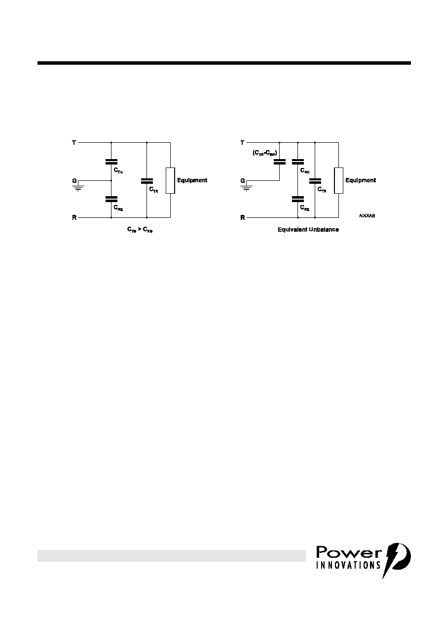
longitudinal balance
Figure 35 shows a three terminal TISP
Æ
with its equivalent "delta" capacitance. Each capacitance, C
TG
, C
RG
and C
TR
, is the true terminal pair capacitance measured with a three terminal or guarded capacitance bridge.
If wire R is biased at a larger potential than wire T then C
TG
> C
RG
. Capacitance C
TG
is equivalent to a
capacitance of C
RG
in parallel with the capacitive difference of (C
TG
- C
RG
). The line capacitive unbalance is
due to (C
TG
- C
RG
) and the capacitance shunting the line is C
TR
+ C
RG
/2 .
Figure 35.
All capacitance measurements in this data sheet are three terminal guarded to allow the designer to
accurately assess capacitive unbalance effects. Simple two terminal capacitance meters (unguarded third
terminal) give false readings as the shunt capacitance via the third terminal is included.
TISP7125F3, TISP7150F3, TISP7180F3, TISP7240F3, TISP7260F3,
TISP7290F3, TISP7320F3, TISP7350F3, TISP7380F3
TRIPLE BIDIRECTIONAL THYRISTOR OVERVOLTAGE PROTECTORS
20
MARCH 1994 - REVISED MARCH 2000
P R O D U C T I N F O R M A T I O N
typical circuits
Figure 36. PROTECTION MODULE
Figure 37. ISDN PROTECTION
Figure 38. LINE CARD RING/TEST PROTECTION
PROTECTED
EQUIPMENT
AI7XBP
TISP7xxxF3
Th3
Th2
Th1
R1a
R1b
RING
WIRE
TIP
WIRE
F1a
F1b
GDTb
GDTa
R1a
R1b
AI7XBM
SIGNAL
D.C.
Th3
Th2
Th1
TISP7150F3
TEST
RELAY
RING
RELAY
SLIC
RELAY
TEST
EQUIP-
MENT
RING
GENERATOR
S1a
S1b
R1a
R1b
RING
WIRE
TIP
WIRE
Th3
Th2
Th1
Th4
Th5
SLIC
SLIC
PROTECTION
RING/TEST
PROTECTION
OVER-
CURRENT
PROTECTION
S2a
S2b
S3a
S3b
V
BAT
C1
220 nF
AI7XBN
TISP6xxxx,
TISPPBLx,
ΩTISP6NTP2
COORDIN-
ATION
RESISTANCE
TISP7xxxF3
21
MARCH 1994 - REVISED MARCH 2000
TISP7125F3, TISP7150F3, TISP7180F3, TISP7240F3, TISP7260F3,
TISP7290F3, TISP7320F3, TISP7350F3, TISP7380F3
TRIPLE BIDIRECTIONAL THYRISTOR OVERVOLTAGE PROTECTORS
P R O D U C T I N F O R M A T I O N
MECHANICAL DATA
D008
plastic small-outline package
This small-outline package consists of a circuit mounted on a lead frame and encapsulated within a plastic
compound. The compound will withstand soldering temperature with no deformation, and circuit performance
characteristics will remain stable when operated in high humidity conditions. Leads require no additional
cleaning or processing when used in soldered assembly.
5,21 (0.205)
4,60 (0.181)
NOTES: A. Leads are within 0,25 (0.010) radius of true position at maximum material condition.
B. Body dimensions do not include mold flash or protrusion.
C. Mold flash or protrusion shall not exceed 0,15 (0.006).
D. Lead tips to be planar within ±0,051 (0.002).
1,75 (0.069)
1,35 (0.053)
6,20 (0.244)
5,80 (0.228)
5,00 (0.197)
4,80 (0.189)
D008
8
7
6
5
4
3
2
1
4,00 (0.157)
3,81 (0.150)
7∞ NOM
3 Places
7∞ NOM
4 Places
0,51 (0.020)
0,36 (0.014)
8 Places
Pin Spacing
1,27 (0.050)
(see Note A)
6 Places
1,12 (0.044)
0,51 (0.020)
4∞ ± 4∞
0,79 (0.031)
0,28 (0.011)
0,203 (0.008)
0,102 (0.004)
ALL LINEAR DIMENSIONS ARE IN MILLIMETERS AND PARENTHETICALLY IN INCHES
8-pin Small Outline Microelectronic Standard
Package MS-012, JEDEC Publication 95
0,50 (0.020)
0,25 (0.010)
x 45∞NOM
0,229 (0.0090)
0,190 (0.0075)
MDXXAAC
INDEX

TISP7125F3, TISP7150F3, TISP7180F3, TISP7240F3, TISP7260F3,
TISP7290F3, TISP7320F3, TISP7350F3, TISP7380F3
TRIPLE BIDIRECTIONAL THYRISTOR OVERVOLTAGE PROTECTORS
22
MARCH 1994 - REVISED MARCH 2000
P R O D U C T I N F O R M A T I O N
MECHANICAL DATA
D008
tape dimensions
D008 Package (8-pin Small Outline) Single-Sprocket Tape
ALL LINEAR DIMENSIONS IN MILLIMETERS
6,30
6,50
11,70
12,30
5,40
5,60
1,50
1,60
3,90
4,10
7,90
8,10
1,95
2,05
0,8 MIN.
0 MIN.
0,40
2,0
2,2
Direction of Feed
¯ 1,5 MIN.
Carrier Tape
Embossment
Cover
Tape
NOTES: A. Taped devices are supplied on a reel of the following dimensions:-
Reel diameter:
330 +0,0/-4,0 mm
Reel hub diameter:
100 ±2,0 mm
Reel axial hole:
13,0 ±0,2 mm
B. 2500 devices are on a reel.
MDXXATB
23
MARCH 1994 - REVISED MARCH 2000
TISP7125F3, TISP7150F3, TISP7180F3, TISP7240F3, TISP7260F3,
TISP7290F3, TISP7320F3, TISP7350F3, TISP7380F3
TRIPLE BIDIRECTIONAL THYRISTOR OVERVOLTAGE PROTECTORS
P R O D U C T I N F O R M A T I O N
MECHANICAL DATA
P008
plastic dual-in-line package
This dual-in-line package consists of a circuit mounted on a lead frame and encapsulated within a plastic
compound. The compound will withstand soldering temperature with no deformation, and circuit performance
characteristics will remain stable when operated in high humidity conditions The package is intended for
insertion in mounting-hole rows on 7,62 (0.300) centres. Once the leads are compressed and inserted,
sufficient tension is provided to secure the package in the board during soldering. Leads require no additional
cleaning or processing when used in soldered assembly.
ALL LINEAR DIMENSIONS IN MILLIMETERS AND PARANTHETICALLY IN INCHES
0,53 (0.021)
0,38 (0.015)
8 Places
1,78 (0.070) MAX
4 Places
6,60 (0.260)
6,10 (0.240)
P008
8,23 (0.324)
7,62 (0.300)
9,75 (0.384)
9,25 (0.364)
2,54 (0.100) Typical
(see Note A)
6 Places
5,08 (0.200)
MAX
3,17 (0.125)
MIN
0,51 (0.020)
MIN
3
1
2
4
8
7
6
5
Seating
Plane
9,40 (0.370)
8,38 (0.330)
0,36 (0.014)
0,20 (0.008)
NOTES: A. Each pin centreline is located within 0,25 (0.010) of its true longitudinal position.
B. Dimensions fall within JEDEC MS001 - R-PDIP-T, 0.300" Dual-In-Line Plastic Family.
C. Details of the previous dot index P008 package style, drawing reference MDXXABA, are given in the earlier publications.
MDXXCF
Index
Notch

TISP7125F3, TISP7150F3, TISP7180F3, TISP7240F3, TISP7260F3,
TISP7290F3, TISP7320F3, TISP7350F3, TISP7380F3
TRIPLE BIDIRECTIONAL THYRISTOR OVERVOLTAGE PROTECTORS
24
MARCH 1994 - REVISED MARCH 2000
P R O D U C T I N F O R M A T I O N
MECHANICAL DATA
SL003
3-pin plastic single-in-line package
This single-in-line package consists of a circuit mounted on a lead frame and encapsulated within a plastic
compound. The compound will withstand soldering temperature with no deformation, and circuit performance
characteristics will remain stable when operated in high humidity conditions. Leads require no additional
cleaning or processing when used in soldered assembly.
ALL LINEAR DIMENSIONS IN MILLIMETERS AND PARANTHETICALLY IN INCHES
2,54 (0.100) Typical
(see Note A)
2 Places
8,31 (0.327)
MAX
SL003
4,267 (0.168)
MIN
1,854 (0.073)
MAX
0,711 (0.028)
0,559 (0.022)
3 Places
12,9 (0.492)
MAX
6,60 (0.260)
6,10 (0.240)
2
1
3
0,356 (0.014)
0,203 (0.008)
3,40 (0.134)
3,20 (0.126)
9,75 (0.384)
9,25 (0.364)
NOTES: A. Each pin centreline is located within 0,25 (0.010) of its true longitudinal position.
B. Body molding flash of up to 0,15 (0.006) may occur in the package lead plane.
C. Details of the previous dot index SL003 style, drawing reference MDXXAD, are given in the earlier publications.
MDXXCE
Index
Notch

25
MARCH 1994 - REVISED MARCH 2000
TISP7125F3, TISP7150F3, TISP7180F3, TISP7240F3, TISP7260F3,
TISP7290F3, TISP7320F3, TISP7350F3, TISP7380F3
TRIPLE BIDIRECTIONAL THYRISTOR OVERVOLTAGE PROTECTORS
P R O D U C T I N F O R M A T I O N
IMPORTANT NOTICE
Power Innovations Limited (PI) reserves the right to make changes to its products or to discontinue any semiconductor product
or service without notice, and advises its customers to verify, before placing orders, that the information being relied on is
current.
PI warrants performance of its semiconductor products to the specifications applicable at the time of sale in accordance with
PI's standard warranty. Testing and other quality control techniques are utilized to the extent PI deems necessary to support this
warranty. Specific testing of all parameters of each device is not necessarily performed, except those mandated by government
requirements.
PI assumes no liability for applications assistance, customer product design, software performance, or infringement of patents
or services described herein. Nor is any license, either express or implied, granted under any patent right, copyright, design
right, or other intellectual property right of PI covering or relating to any combination, machine, or process in which such
semiconductor products or services might be or are used.
PI SEMICONDUCTOR PRODUCTS ARE NOT DESIGNED, INTENDED, AUTHORISED, OR WARRANTED TO BE SUITABLE
FOR USE IN LIFE-SUPPORT APPLICATIONS, DEVICES OR SYSTEMS.
Copyright © 2000, Power Innovations Limited