Specifications are subject to change without notice.
306
MARCH 1994 - REVISED OCTOBER 2000
TISP7xxxF3
(MV, HV) Overvoltage Protector Series
TISP7125F3 THRU TISP7180F3,
TISP7240F3 THRU TISP7380F3
MEDIUM & HIGH-VOLTAGE TRIPLE ELEMENT
BIDIRECTIONAL THYRISTOR OVERVOLTAGE PROTECTORS
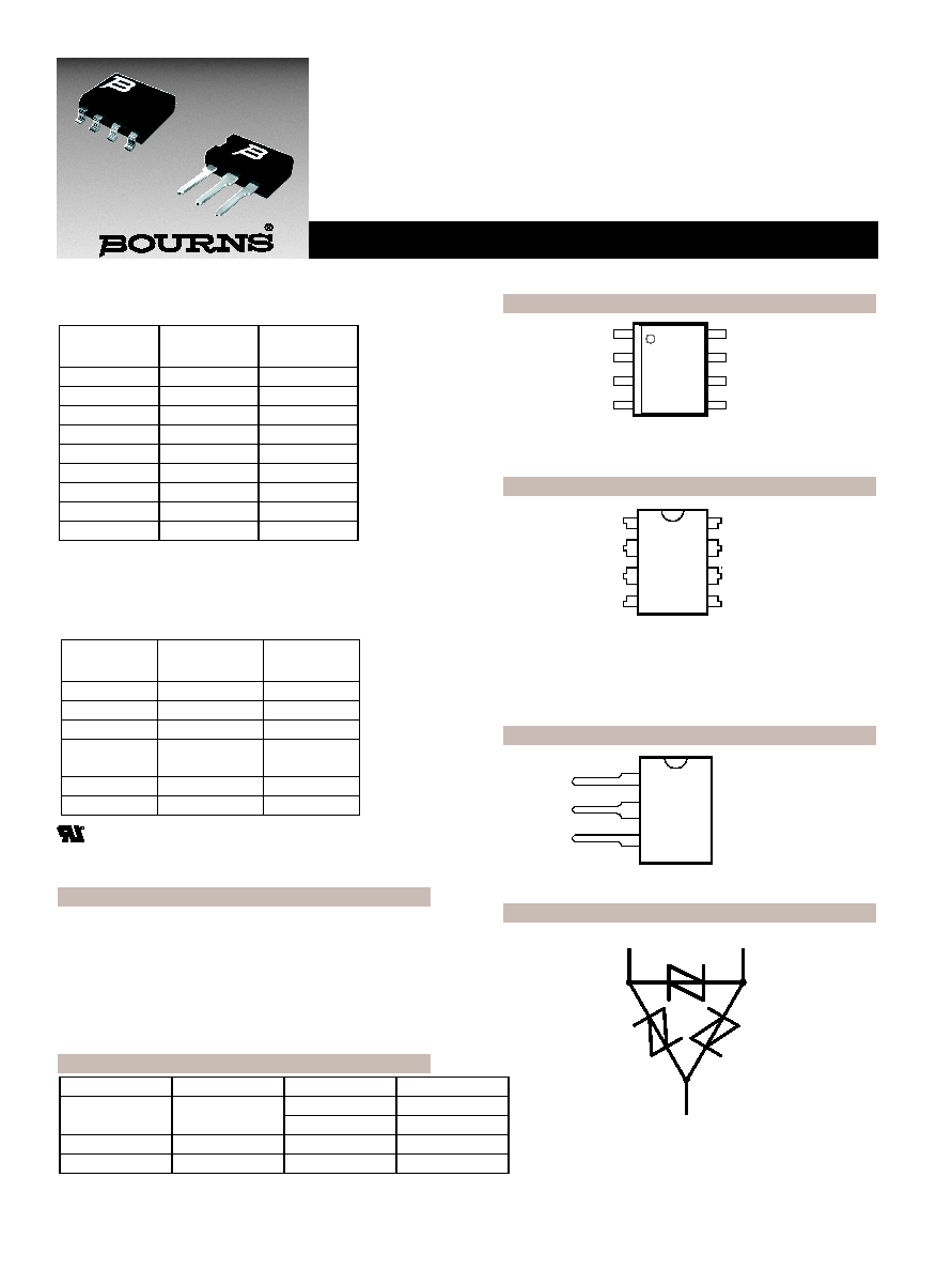
Device Symbol
SL Package (Top View)
P Package (Top View)
Device
V
DRM
V
V
(BO)
V
`7125F3 100
125
`7150F3 120
150
`7180F3 145
180
`7240F3 180
240
`7260F3 200
260
`7290F3 220
290
`7320F3 240
320
`7350F3 275
350
`7380F3
270
380
For new designs use `7350F3 instead of `7380F3
Waveshape
Standard
I
TSP
A
2/10
GR-1089-CORE
190
8/20
IEC 61000-4-5
175
10/160
FCC Part 68
110
10/700
FCC Part 68
ITU-T K.20/21
70
10/560
FCC Part 68
50
10/1000
GR-1089-CORE
45
Patented Ion-Implanted Breakdown Region
- Precise DC and Dynamic Voltages
Planar Passivated Junctions
- Low Off-State Current.................................<10
µA
Rated for International Surge Wave Shapes
- Single and Simultaneous Impulses
How To Order
Device
Package
Carrier
Order #
TISP7xxxF3
D, Small-outline
Tape and Reel
TISP7xxxF3DR
Tube
TISP7xxxF3D
TISP7xxxF3
P, Plastic DIP
Tube
TISP7xxxF3P
TISP7xxxF3
SL, Single-in-line
Tube
TISP7xxxF3SL
Description
D Package (Top View)
The TISP7xxxF3 series are 3-point overvoltage protectors
designed for protecting against metallic (differential mode) and
simultaneous longitudinal (common mode) surges. Each terminal
pair has the same voltage limiting values and surge current
capability. This terminal pair surge capability ensures that the
protector can meet the simultaneous longitudinal surge require-
ment which is typically twice the metallic surge requirement.
.............................................. UL Recognized Component
1
2
3
4
5
6
7
8
G
NU
NU
G
NC
T
R
NC
R
NC
T
NC
G
NU
NU
G
1
2
3
4
5
6
7
8
NC - No internal connection.
NU - Non-usable; no external electrical connection should be made
to these pins.
Specified ratings require connection of pins 5 and 8.
MD1XAB
1
2
3
T
G
R
G
T
R
SD7XAB
Terminals T, R and G correspond to the
alternative line designators of A, B and C

Specifications are subject to change without notice.
307
MARCH 1994 - REVISED OCTOBER 2000
Description (continued)
TISP7xxxF3 (MV, HV) Overvoltage Protector Series
Absolute Maximum Ratings, TA = 25 ∞C (Unless Otherwise Noted)
Each terminal pair has a symmetrical voltage-triggered thyristor characteristic. Overvoltages are initially clipped by breakdown clamping until
the voltage rises to the breakover level, which causes the device to crowbar into a low-voltage on state. This low-voltage on state causes the
current resulting from the overvoltage to be safely diverted through the device. The high crowbar holding current prevents d.c. latchup as the
diverted current subsides.These protectors are guaranteed to voltage limit and withstand the listed lightning surges in both polarities.
These medium and high voltage devices are offered in nine voltage variants to meet a range of battery and ringing voltage requirements. They
are guaranteed to suppress and withstand the listed international lightning surges on any terminal pair. Similar devices with working voltages of
58 V and 66 V are detailed in the TISP7072F3, TISP7082F3 data sheet.
Rating
Symbol
Value
Unit
Repetitive peak off-state voltage, 0
∞C < T
A
< 70
∞C
`7125F3
`7150F3
`7180F3
`7240F3
`7260F3
`7290F3
`7320F3
`7350F3
`7380F3
V
DRM
100
120
145
180
200
220
240
275
270
V
Non-repetitive peak on-state pulse current (see Notes 1 and 2)
I
PPSM
A
1/2 (Gas tube differential transient, 1/2 voltage wave shape)
330
2/10 (Telcordia GR-1089-CORE, 2/10 voltage wave shape)
190
1/20 (ITU-T K.22, 1.2/50 voltage wave shape, 25
resistor)
100
8/20 (IEC 61000-4-5, combination wave generator, 1.2/50 voltage wave shape)
175
10/160 (FCC Part 68, 10/160 voltage wave shape)
110
4/250 (ITU-T K.20/21, 10/700 voltage wave shape, simultaneous)
95
0.2/310 (CNET I 31-24, 0.5/700 voltage wave shape)
70
5/310 (ITU-T K.20/21, 10/700 voltage wave shape, single)
70
5/320 (FCC Part 68, 9/720 voltage wave shape, single)
70
10/560 (FCC Part 68, 10/560 voltage wave shape)
50
10/1000 (Telcordia GR-1089-CORE, 10/1000 voltage wave shape)
45
Non-repetitive peak on-state current, 0
∞C < T
A
< 70
∞C (see Notes 1 and 3)
50 Hz,
1 s
D Package
P Package
SL Package
I
TSM
4.3
5.7
7.1
A
Initial rate of rise of on-state current,
Linear current ramp, Maximum ramp value < 38 A
di
T
/dt
250
A/
µs
Junction temperature
T
J
-65 to +150
∞C
Storage temperature range
T
stg
-65 to +150
∞C
NOTES: 1.
2. See Thermal Information for derated I
PPSM
values 0
∞C < T
A
< 70
∞C and Applications Information for details on wave shapes.
3. Above 70
∞C, derate I
TSM
linearly to zero at 150
∞C lead temperature.
Initially, the TISP device must be in thermal equilibrium at the specified T . The impulse may be repeated after the TISP device
returns to its initial conditions. The rated current values may be applied either to the R to G or to the T to G or to the T to R
terminals. Additionally, both R to G and T to G may have their rated current values applied simultaneously (In this case the total
G terminal current will be twice the above rated current values).
A
Æ
Æ
Specifications are subject to change without notice.
308
MARCH 1994 - REVISED OCTOBER 2000
Electrical Characteristics for all Terminal Pairs, TA = 25 ∞C (Unless Otherwise Noted)
Parameter
Test Conditions
Min
Typ
Max
Unit
I
DRM
Repetitive peak off-
state current
V
D
= V
DRM
, 0
∞C < T
A
< 70
∞C
±10
µA
V
(BO)
Breakover voltage
dv/dt =
±250 V/ms, R
SOURCE
= 300
`7125F3
`7150F3
`7180F3
`7240F3
`7260F3
`7290F3
`7320F3
`7350F3
`7380F3
±125
±150
±180
±240
±260
±290
±320
±350
±380
V
V
(BO)
Impulse breakover
voltage
dv/dt
±1000 V/µs, Linear voltage ramp,
Maximum ramp value =
±500 V
di/dt =
±20 A/µs, Linear current ramp,
Maximum ramp value =
±10 A
`7125F3
`7150F3
`7180F3
`7240F3
`7260F3
`7290F3
`7320F3
`7350F3
`7380F3
±143
±168
±198
±269
±289
±319
±349
±379
±409
V
I
(BO)
Breakover current
dv/dt =
±250 V/ms, R
SOURCE
= 300
±0.1
±0.8
A
V
T
On-state voltage
I
T
=
±5 A, t
W
= 100
µs
±5
V
I
H
Holding current
I
T
=
±5 A, di/dt = - /+30 mA/ms
±0.15
A
dv/dt
Critical rate of rise of
off-state voltage
Linear voltage ramp, Maximum ramp value < 0.85V
DRM
±5
kV/
µs
I
D
Off-state current
V
D
=
±50 V
±10
µA
C
off
Off-state capacitance
f = 1 MHz,
V
d
= 1 V rms, V
D
= 0
f = 1 MHz,
V
d
= 1 V rms, V
D
= -1 V
f = 1 MHz,
V
d
= 1 V rms, V
D
= -2 V
f = 1 MHz,
V
d
= 1 V rms, V
D
= -5 V
f = 1 MHz,
V
d
= 1 V rms, V
D
= -50 V
f = 1 MHz,
V
d
= 1 V rms, V
D
= -100 V
f = 1 MHz,
V
d
= 1 V rms, V
DTR
= 0
(see Note 4)
`7125 thru `7180
`7240 thru `7380
`7125 thru `7180
`7240 thru `7380
`7125 thru `7180
`7240 thru `7380
`7125 thru `7180
`7240 thru `7380
`7125 thru `7180
`7240 thru `7380
`7125 thru `7180
`7240 thru `7380
`7125 thru `7180
`7240 thru `7380
37
31
40
34
36
30
31
24
17
13
14
10
20
17
48
41
52
44
47
39
40
31
23
17
18
13
27
23
pF
NOTE
4: Three-terminal guarded measurement, unmeasured terminal voltage bias is zero. First six capacitance values, with bias V
D
, are
for the R-G and T-G terminals only. The last capacitance value, with bias V
DTR
, is for the T-R terminals.
Thermal Characteristics
TISP7xxxF3 (MV, HV) Overvoltage Protector Series
Parameter
Test Conditions
Min
Typ
Max
Unit
R
JA
Junction to free air thermal resistance
P
tot
= 0.8 W, T
A
= 25
∞C
5 cm
2
, FR4 PCB
D Package
160
∞C/W
P Package
100
SL Package
135

Specifications are subject to change without notice.
309
MARCH 1994 - REVISED OCTOBER 2000
Parameter Measurement Information
TISP7xxxF3 (MV, HV) Overvoltage Protector Series
Figure 1. Voltage-Current Characteristic for T and R Terminals
T and G and R and G Measurements are Referenced to the G Terminal
T and R Measurements are Referenced to the R Terminal
-v
V
DRM
I
DRM
V
D
I
H
I
TSM
I
TSP
V
(BO)
I
(BO)
I
D
Quadrant I
Switching
Characteristic
+v
+i
V
(BO)
I
(BO)
V
DRM
I
DRM
V
D
I
D
I
H
I
TSM
I
TSP
-i
Quadrant III
Switching
Characteristic
PMXXAAA

Specifications are subject to change without notice.
310
MARCH 1994 - REVISED OCTOBER 2000
Typical Characteristics - R and G, or T and G Terminals
TISP7xxxF3 (MV, HV) Overvoltage Protector Series
Figure 2.
Figure 3.
Figure 4.
Figure 5.
T
J
- Junction Temperature -
∞C
T
J
- Junction Temperature -
∞C
T
J
- Junction Temperature -
∞C
-25
0
25
50
75
100
125
150
I
D
-
Off-S
mA
tate
Cu
rren
t
-
0∑001
0∑01
0∑1
0∑001
0∑01
0∑1
1
10
100
TC7MAC
V
D
= -50 V
V
D
= 50 V
-25
0
25
50
75
100
125
150
I
D
- Off-
S
t
at
e Current -
1
10
100
TC7HAC
V
D
= -50 V
V
D
= 50 V
-25
0
25
50
75
100
125
150
0.9
1.0
1.1
1.2
TC7MAE
V
(BO)
V
(BR)
V
(BR)M
Positive Polarity
Normalized to V
(BR)
I
(BR)
= 1 mA and 25
∞C
T
J
- Junction Temperature -
∞C
1 mA and 25
∞C
-25
0
25
50
75
100
125
150
Normalized Breakdown Voltages
0.9
1.0
1.1
1.2
TC7HAE
V
(BO)
V
(BR)
V
(BR)M
Positive Polarity
Normalized to V
(BR)
I
(BR)
=
TISP7125F3 THRU TISP7180F3
OFF-STATE CURRENT
vs
JUNCTION TEMPERATURE
TISP7240F3 THRU TISP7380F3
OFF-STATE CURRENT
vs
JUNCTION TEMPERATURE
NORMALIZED BREAKDOWN VOLTAGES
vs
JUNCTION TEMPERATURE
NORMALIZED BREAKDOWN VOLTAGES
vs
JUNCTION TEMPERATURE
mA
1 mA and 25
∞C
Normalized Breakdown Voltages