Specifications are subject to change without notice.
1
JULY 2000 - REVISED FEBRUARY 2002
TISP8250 Unidirectional P-Gate Protector
TISP8250
UNIDIRECTIONAL THYRISTOR
OVERVOLTAGE AND OVERCURRENT PROTECTORS
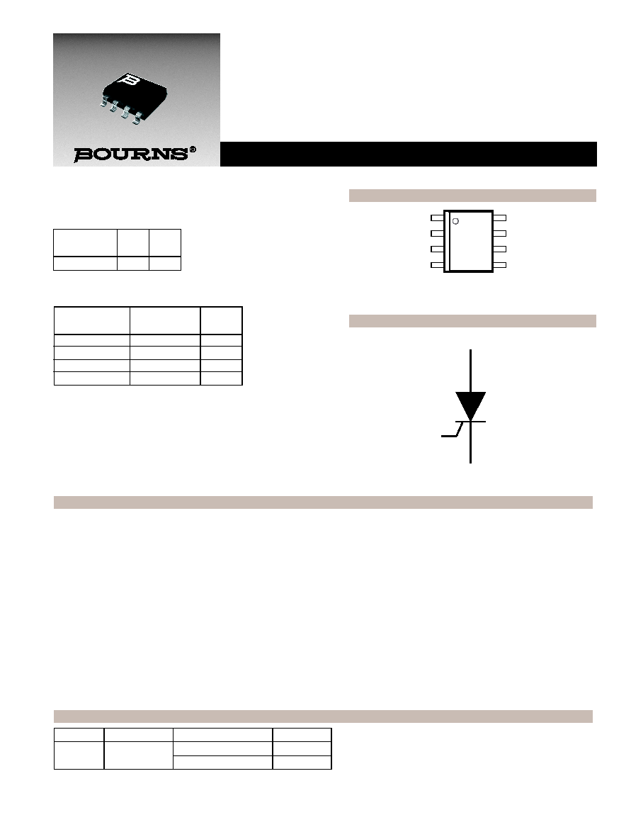
Device Symbol
Telecommunication System 30 A 10/1000 Protectors
Ion-Implanted Breakdown Region
- Precise and Stable Voltage
Rated for International Surge Wave Shapes
How To Order
D Package (Top View)
Description
The TISP8250 is a P-gate reverse-blocking thyristor (SCR) designed for the protection of telecommunications equipment against
overvoltages and overcurrents on the telephone line caused by lightning, a.c. power contact and induction. The fixed voltage and current
triggered modes make the TISP8250 particularly suitable for the protection of ungrounded customer premise equipment. Connected
across the d.c. side of a telephone set polarity bridge, in fixed voltage mode these devices can protect the ringer in the on-hook condition.
In an off-hook condition, either the fixed voltage or current triggered modes can protect the following telephone electronics.
Without external gate activation, the TISP8250 is a fixed voltage protector. The maximum working voltage without clipping is 250 V and the
protection voltage is 340 V. Lower values of protection voltage may be set by connecting an avalanche breakdown diode of less than 250 V
between the TISP8250 gate and anode (see Figure 2.)
By connecting a small value resistor in series with the line conductor and connecting the TISP8250 gate cathode terminals in parallel with
the resistor, conductor overcurrents can gate trigger the TISP8250 into conduction.
Overvoltages are initially clipped by breakdown clamping until the voltage rises to the breakover level, which causes the device to crowbar
into a low-voltage on state. Overcurrents develop sufficient voltage across the external gate-cathode resistor to trigger the device into a
low-voltage on state. This low-voltage on state causes the current resulting from the overstress to be safely diverted through the device.
The high crowbar holding current prevents d.c. latchup as the diverted current subsides.
DEVICE
V
DRM
V
V
(BO)
V
`8250
250
340
Waveshape
Standard
I
PPSM
A
2/10
GR-1089-CORE
75
10/700
ITU-T K.20/21
40
10/1000
GR-1089-CORE
30
0.5/700
CNET I 31-24
40
1
2
3
4
5
6
7
8
A
A
A
A
NC
G
K
NC
NC - No internal connection
MD8XAAA
K
G
SD8XAA
A
Functional Replacement for TPP25011
Device
Package
Carrier
Order As
TISP8250
D, Small-outline
Embossed Tape Reeled
TISP8250DR
Tube
TISP8250D

Specifications are subject to change without notice.
2
JULY 2000 - REVISED FEBRUARY 2002
Electrical Characteristics, TJ = 25 ∞C (Unless Otherwise Noted)
TISP8250 Unidirectional P-Gate Protector
Absolute Maximum Ratings, TJ = 25 ∞C (Unless Otherwise Noted)
Thermal Characteristics
Rating
Symbol
Value
Unit
Repetitive peak off-state voltage, (see Note 1)
V
DRM
250
V
Non-repetitive peak on-state pulse current (see Notes 2, 3 and 4)
I
PPSM
A
2/10
µs (GR-1089-CORE, 2/10 µs voltage wave shape)
75
0.2/310
µs (CNET I 31-24, 0.5/700 µs voltage wave shape)
40
5/310
µs (ITU-T K.20/21, 10/700 µs voltage wave shape)
40
5/310
µs (FTZ R12, 10/700 µs voltage wave shape)
40
10/1000
µs (GR-1089-CORE, 10/1000 µs voltage wave shape)
30
Non-repetitive peak on-state current (see Notes 2, 3 and 4)
I
TSM
A
10 ms (50 Hz) half sine wave
1 s (50 Hz) rectified sine wave
1000 s (50 Hz) rectified sine wave
5
3.5
0.7
Junction temperature
T
J
-40 to +150
∞C
Storage temperature range
T
stg
-65 to +150
∞C
NOTES: 1. For voltage values at lower temperatures derate at 0.13 %/
∞C.
2. Initially, the TISP8250 must be in thermal equilibrium with T
J
= 25
∞C.
3. The surge may be repeated after the TISP8250 returns to its initial conditions.
4. EIA/JESD51-2 environment and EIA/JESD51-3 PCB with standard footprint dimensions connected with 5 A rated printed wiring
track widths. Derate current values at -0.61 %/
∞C for ambient temperatures above 25 ∞C.
Parameter
Test Conditions
Min
Typ
Max
Unit
I
DRM
Repetitive peak off-
state current
V
D
= V
DRM
T
A
= 25
∞C
5
10
µA
T
A
= 85
∞C
V
(BO)
Breakover voltage
dv/dt = 250 V/ms, R
SOURCE
= 300
340
V
I
(BO)
Forward voltage
dv/dt = 250 V/ms, R
SOURCE
= 300
15
200
mA
I
H
Holding current
I
T
= 5 A, di/dt = -30 mA/ms
180
mA
V
GK
Gate-cathode voltage
I
G
= 30 mA
0.6
1.2
V
I
GT
Gate trigger current
V
AK
= 100 V
40
mA
I
D
Off-state current
V
D
= 60 V
5
µA
C
off
Off-state capacitance
f = 1 MHz, V
d
= 1 V rms, V
D
= 5 V
100
pF
Parameter
Test Conditions
Min
Typ
Max
Unit
R
JA
Junctio n to free air thermal resistance
EIA/JESD51-3 PCB, I
T
= I
TSM(1000)
,
T
A
= 25
∞C, (see Note 5)
170
∞C/W
NOTE 5: EIA/JESD51-2 environment and PCB has standard footprint dimensions connected with 5 A rated printed wiring track widths.
Specifications are subject to change without notice.
3
JULY 2000 - REVISED FEBRUARY 2002
Parameter Measurement Information
TISP8250 Unidirectional P-Gate Protector
Figure 1. Voltage-Curr ent Characteristic for A and K Terminals
All Measurements are Referenced to the K Terminal
PM8XAAA
Quadrant I
Anode Positive
Switching Characteristic
Quadrant III
Anode Negative
Reverse Characteristic
I
H
+v
-i
-v
V
DRM
+i
V
(BO)
V
D
I
D
I
DRM
I
(BO)
Figure 2. Overvoltage Protection Circuit
K
G
AI8XACA
A
Avalanche
diode
V
(BR)
< 250 V
TISP-
8250

Specifications are subject to change without notice.
4
JULY 2000 - REVISED FEBRUARY 2002
MECHANICAL DATA
TISP8250 Unidirectional P-Gate Protector
Device Symbolization Code
Devices will be coded as below.
Device
Symbolization
Code
TISP8250
8250

Specifications are subject to change without notice.
5
JULY 2000 - REVISED FEBRUARY 2002
This small-outline package consists of a circuit mounted on a lead frame and encapsulated within a plastic compound. The compound will
withstand soldering temperature with no deformation, and circuit performance characteristics will remain stable when operated in high
humidity conditions. Leads require no additional cleaning or processing when used in soldered assembly.
D008 Plastic Small-outline Package
TISP8250 Unidirectional P-Gate Protector
MECHANICAL DATA
NOTES: A. Leads are within 0.25 (0.010) radius of true position at maximum material condition.
B. Body dimensions do not include mold flash or protrusion.
C. Mold flash or protrusion shall not exceed 0.15 (0.006).
D. Lead tips to be planar within
±0.051 (0.002).
D008
8
7
6
5
4
3
2
1
8-pin Small Outline Microelectronic Standard
Package MS-012, JEDEC Publication 95
MDXXAA E
INDEX
4.80 - 5.00
(0.189 - 0.197)
5.80 - 6.20
(0.228 - 0.244)
3.81 - 4.00
(0.150 - 0.157)
1.35 - 1.75
(0.053 - 0.069)
0.102 - 0.203
(0.004 - 0.008)
0.28 - 0.79
(0.011 - 0.031)
0.51 - 1.12
(0.020 - 0.044)
4.60 - 5.21
(0.181 - 0.205)
0.36 - 0.51
(0.014 - 0.020)
0.25 - 0.50
(0.010 - 0.020)
0.190 - 0.229
(0.0075 - 0.0090)
Pin Spacing
1.27
(0.050)
(see Note A)
6 places
x 45
∞ N0M
8 Places
7
∞ NOM
4 Places
7
∞ NOM
3 Places
4
∞ ± 4 ∞
DIMENSIONS ARE:
MM
(INCHES)

Specifications are subject to change without notice.
6
JULY 2000 - REVISED FEBRUARY 2002
MECHANICAL DATA
TISP8250 Unidirectional P-Gate Protector
D008 Tape DImensions
0.8
(.03)
1.50
(.059)
3.90 - 4.10
(.154 - .161)
5.40 - 5.60
(.213 - .220)
1.95 - 2.05
(.077 - .081)
7.90 - 8.10
(.311 - .319)
6.30 - 6.50
(.248 - .256)
11.70 - 12.30
(.461 - .484)
D008 Package (8-pin Small Outline) Single-Sprocket Tape
Direction of Feed
¯ MIN.
Carrier Tape
Embossment
Cover
Tape
NOTES: A. Taped devices are supplied on a reel of the following dimensions:-
Reel diameter:
Reel hub diameter:
Reel axial hole:
B. 2500 devices are on a reel.
MDXXATC
DIMENSIONS ARE:
MM
(INCHES)
330 +0.0/-4.0
(12.99 +0.0/-.157)
100
± 2.0
(3.937
± .079)
13.0
± 0.2
(.512
± .008)
0 MIN.
MIN.
0.40
(.016)
2.0 - 2.2
(.079 - .087)
1.50 - 1.60
(.059 - .063)
"TISP" is a trademark of Power Innovations, Ltd., a Bourns Company and Registered in U.S. Patent and Trademark Office.
"Bourns" is a registered trademark of Bourns, Inc. in the U.S. and other countries.
COPYRIGHT© 2002, BOURNS, INC. LITHO IN U.S.A. 06/02 e/PI0222
Reliable Electronic Solutions
North America:
TEL +1-909 781-5500
FAX +1-909 781-5700
bourns.com