PHASE CONTROL THYRISTOR
AT405
Repetitive voltage up to
1200
V
Mean on-state current
305
A
Surge current
2.8
kA
FINAL SPECIFICATION
gen 03 - ISSUE : 05
Symbol
Characteristic
Conditions
Tj
[°C]
Value
Unit
BLOCKING
V
RRM
Repetitive peak reverse voltage
125
1200
V
V
RSM
Non-repetitive peak reverse voltage
125
1300
V
V
DRM
Repetitive peak off-state voltage
125
1200
V
I
RRM
Repetitive peak reverse current
V=VRRM
125
30
mA
I
DRM
Repetitive peak off-state current
V=VDRM
125
30
mA
CONDUCTING
I
T (AV)
Mean on-state current
180° sin, 50 Hz, Th=55°C, double side cooled
305
A
I
T (AV)
Mean on-state current
180° sin, 50 Hz, Tc=85°C, double side cooled
245
A
I
TSM
Surge on-state current
sine wave, 10 ms
125
2.8
kA
I² t
I² t
without reverse voltage
39 x1E3
A²s
V
T
On-state voltage
On-state current =
600 A
25
1.88
V
V
T(TO)
Threshold voltage
125
1.0
V
r
T
On-state slope resistance
125
1.900
mohm
SWITCHING
di/dt
Critical rate of rise of on-state current, min.
From 75% VDRM up to 300 A, gate 10V 5ohm
125
200
A/µs
dv/dt
Critical rate of rise of off-state voltage, min.
Linear ramp up to 70% of VDRM
125
500
V/µs
td
Gate controlled delay time, typical
VD=100V, gate source 10V, 10 ohm , tr=.5 µs
25
0.7
µs
tq
Circuit commutated turn-off time, typical
dV/dt = 20 V/µs linear up to 75% VDRM
200
µs
Q rr
Reverse recovery charge
di/dt=-20 A/µs, I= 195 A
125
µC
I rr
Peak reverse recovery current
VR= 50 V
A
I
H
Holding current, typical
VD=5V, gate open circuit
25
300
mA
I
L
Latching current, typical
VD=5V, tp=30µs
25
700
mA
GATE
V
GT
Gate trigger voltage
VD=5V
25
3.5
V
I
GT
Gate trigger current
VD=5V
25
200
mA
V
GD
Non-trigger gate voltage, min.
VD=VDRM
125
0.25
V
V
FGM
Peak gate voltage (forward)
20
V
I
FGM
Peak gate current
8
A
V
RGM
Peak gate voltage (reverse)
5
V
P
GM
Peak gate power dissipation
Pulse width 100 µs
75
W
P
G
Average gate power dissipation
1
W
MOUNTING
R
th(j-h)
Thermal impedance, DC
Junction to heatsink, double side cooled
95
°C/kW
R
th(c-h)
Thermal impedance
Case to heatsink, double side cooled
20
°C/kW
T
j
Operating junction temperature
-30 / 125
°C
F
Mounting force
4.9 / 5.9
kN
Mass
55
g
ORDERING INFORMATION : AT405 S 12
standard specification
VDRM&VRRM/100
POSEICO SPA
POwer SEmiconductors Italian COrporation
POSEICO
POSEICO SPA
Via N. Lorenzi 8, 16152 Genova - ITALY
Tel. ++ 39 010 6556234 - Fax ++ 39 010 6557519
Sales Office:
Tel. ++ 39 010 6556775 - Fax ++ 39 010 6442510

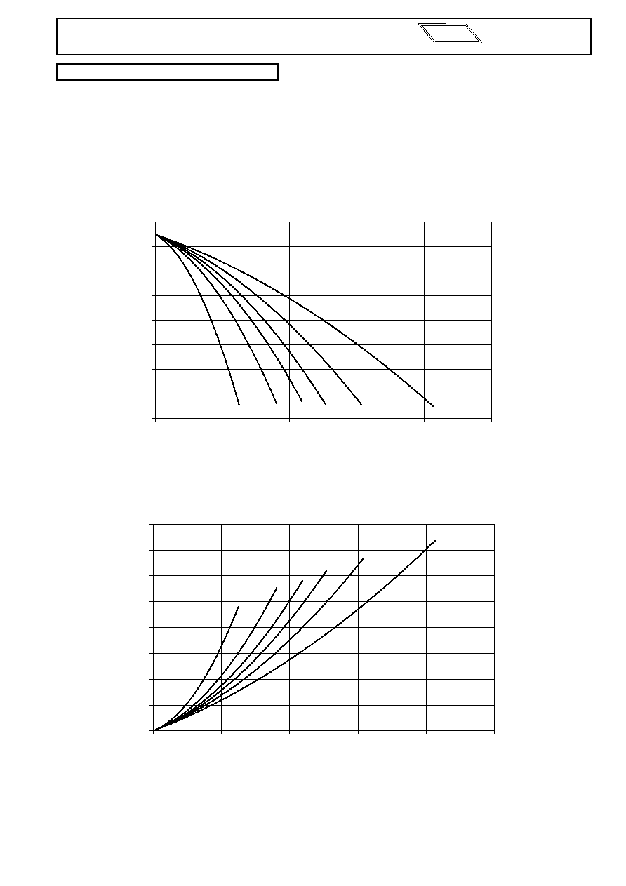
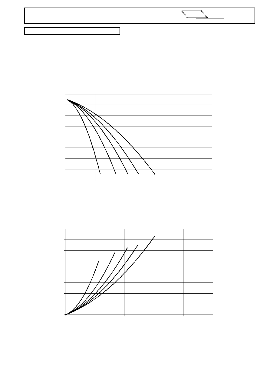
AT405 PHASE CONTROL THYRISTOR
FINAL SPECIFICATION gen 03 - ISSUE : 05
Cathode terminal type DIN 46244 - A 4.8 - 0.8
Gate terminal type AMP 60598 - 1
Distributed by
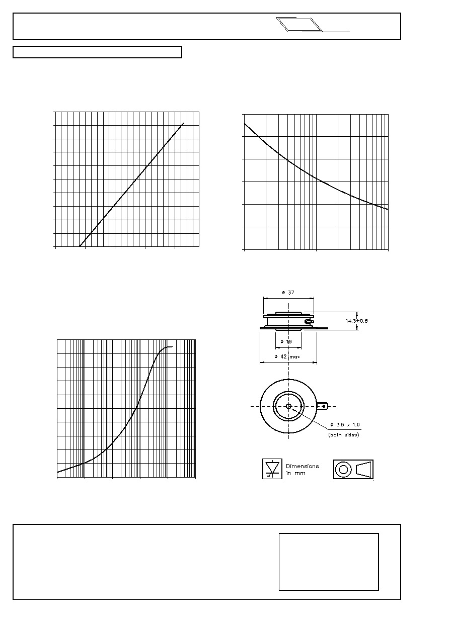
ON-STATE CHARACTERISTIC
Tj = 125 °C
0
100
200
300
400
500
600
700
800
900
1000
0.6
1.1
1.6
2.1
2.6
On-state Voltage [V]
On-state Current [A]
TRANSIENT THERMAL IMPEDANCE
DOUBLE SIDE COOLED
0.0
10.0
20.0
30.0
40.0
50.0
60.0
70.0
80.0
90.0
100.0
0.001
0.01
0.1
1
10
100
t[s]
Zth j-h [°C/kW]
SURGE CHARACTERISTIC
Tj = 125 °C
0
0.5
1
1.5
2
2.5
3
1
10
100
n° cycles
ITSM [kA]
All the characteristics given in this data sheet are guaranteed only with uniform
clamping force, cleaned and lubricated heatsink, surfaces with flatness < .03 mm
and roughness < 2 µm.
In the interest of product improvement POSEICO S.p.A. reserves the right to change
any data given in this data sheet at any time without previous notice.
If not stated otherwise the maximum value of ratings (simbols over shaded
background) and characteristics is reported.
POSEICO SPA
POwer SEmiconductors Italian COrporation
POSEICO


