 | –≠–ª–µ–∫—Ç—Ä–æ–Ω–Ω—ã–π –∫–æ–º–ø–æ–Ω–µ–Ω—Ç: DSP1N5S15 | –°–∫–∞—á–∞—Ç—å:  PDF PDF  ZIP ZIP |
Document Outline
- DC-DC Converters
- Board Mountable
- Briks
- Cassette Style
- Open Frame
- AC-DC Converters
- Board Mountable
- Cassette Style
- Modular Supplies
- Open Frame
- DIN Rail Mountable
- Linear Supplies
- Switching Regulators
- Board Mountable
- Chassis Mountable
- Cassette Style
- Accessory
- Front Panels
- Mounting Supports
- Rack Systems
- Mating Connectors
- Temperature Sensors
- Filter Chokes
- Back Planes
- Technical Information
- english
- deutsch
- franÁais
- nederlands
- Commercial Information
- english
- deutsch
- franÁais
- nederlands
- Image
- Quick Find
- Table of Contents
- Inquiry Form IFC
- english
- deutsch
- franÁais
- nederlands
- Reply and Order Form
- english
- deutsch
- franÁais
- nederlands
- Sales Contacts
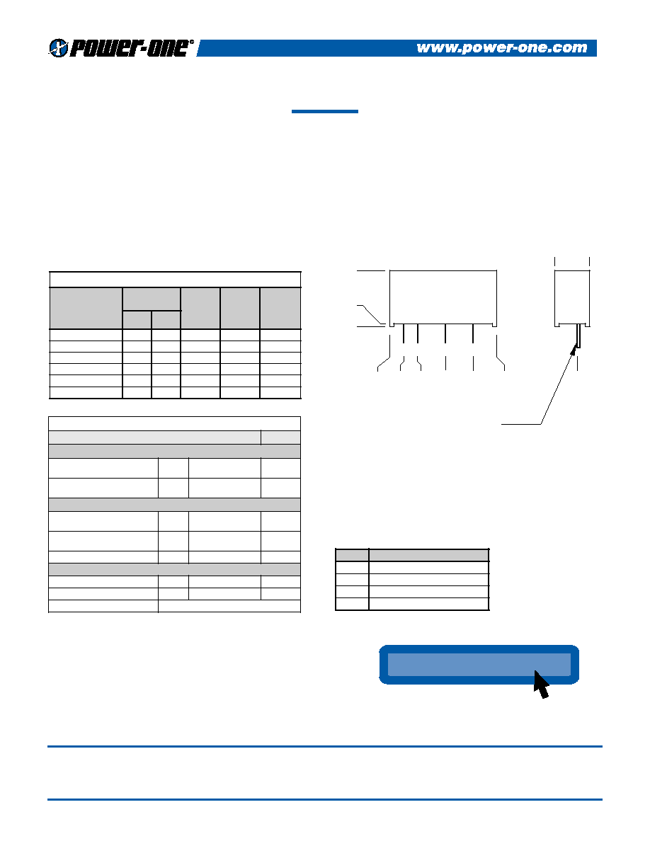
+IN
-IN
-OUT
+OUT
FRONT VIEW
RT
SIDE
VIEW
0.77
0.600
0.400
0.200
0.100
0.000
0.40
0.02
0.000
0.27
0.000
0.09
(2.54)
(5.08)
(10.16)
(15.24)
(19.56)
(0.51)
(10.16)
(6.86)
(2.29)
PINS: 0.02 (0.51) x 0.01 (0.25)
1
2
3
4
LENGTH (TYPICAL): 0.15 (3.81)
DESCRIPTION
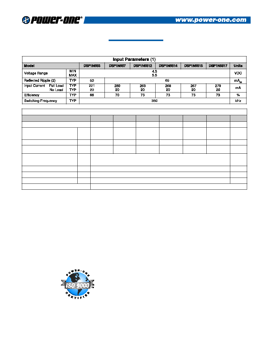
The DSP1 Series is specifically designed to convert a nominal 5
volt input into an isolated output voltage. The semi-regulated
output voltages were designed to allow analog circuits and three
terminal regulators to operate within their most efficient input
voltage range. This series achieves high power densities through
the use of 350KHz fixed frequency switching converters.
FEATURES
∑
Up to 1 Watt Unregulated Output Power
∑
Single In Line Package
∑
Four Terminal Operation
∑
Efficiencies to 75%
∑
350KHz Fixed Frequency Operation
∑
700V Isolation
∑
-40∞C to +85∞C Operation
s
n
o
i
t
a
c
i
f
i
c
e
p
S
l
a
r
e
n
e
G
)
1
(
s
l
e
d
o
M
l
l
A
s
t
i
n
U
n
o
i
t
a
l
o
s
I
e
g
a
t
l
o
V
n
o
i
t
a
l
o
s
I
0
1
t
u
p
t
u
O
o
t
t
u
p
n
I
µ
A
N
I
M
0
0
7
C
D
V
t
u
p
t
u
O
o
t
t
u
p
n
I
e
c
n
a
t
i
c
a
p
a
C
P
Y
T
5
2
F
p
l
a
t
n
e
m
n
o
r
i
v
n
E
c
T
,
e
g
n
a
R
g
n
i
t
a
r
e
p
O
e
s
a
C
(3)
N
I
M
X
A
M
40
-
5
8
+
∞
C
e
g
n
a
R
e
g
a
r
o
t
S
N
I
M
X
A
M
5
5
-
5
0
1
∞
C
)
2
(
e
c
n
a
d
e
p
m
I
l
a
m
r
e
h
T
P
Y
T
8
5
∞
t
t
a
W
/
C
l
a
r
e
n
e
G
)
d
e
t
a
l
u
c
l
a
C
(
F
B
T
M
P
Y
T
0
0
0
,
0
0
7
S
R
H
t
h
g
i
e
W
t
i
n
U
P
Y
T
8
.
2
/
1
.
0
m
g
/
z
o
l
a
i
r
e
t
a
M
e
s
a
C
c
i
t
s
a
l
P
e
v
i
t
c
u
d
n
o
C
n
o
N
Mechanical tolerances unless otherwise noted:
X.XX dimensions: ±0.020 inches
X.XXX dimensions: ±0.010 inches
n
i
P
n
o
i
t
c
n
u
F
1
T
U
P
N
I
+
2
T
U
P
N
I
-
3
T
U
O
-
4
T
U
O
+
NOTES
(1)
All parameters measured at Tc=25∞C, nominal input voltage and full rated load unless otherwise
noted.
(2)
The case Thermal Impedance is specified as the case temperature rise over ambient per package dis-
sipated.
(3)
Derate output power linearly to 0.6 watts from 70∞c to 85∞c.
DSP1 SERIES
SINGLE OUTPUT
t
r
a
h
C
n
o
i
t
c
e
l
e
S
l
e
d
o
M
e
g
n
a
R
t
u
p
n
I
C
D
V
t
u
p
t
u
O
C
D
V
t
u
p
t
u
O
A
m
r
e
w
o
P
W
n
i
M
x
a
M
5
S
5
N
1
P
S
D
5
.
4
5
.
5
5
0
5
1
5
7
.
0
7
S
5
N
1
P
S
D
5
.
4
5
.
5
7
0
4
1
0
.
1
2
1
S
5
N
1
P
S
D
5
.
4
5
.
5
2
1
0
8
0
.
1
4
1
S
5
N
1
P
S
D
5
.
4
5
.
5
4
1
0
7
0
.
1
5
1
S
5
N
1
P
S
D
5
.
4
5
.
5
5
1
5
6
0
.
1
7
1
S
5
N
1
P
S
D
5
.
4
5
.
5
7
1
0
6
0
.
1
www.power-one.com
www.power-one.com
For the Most Up-To-Date Information
24 Hours/Day--7 Days/Week
1
Rev. 04/2000
NUCLEAR AND MEDICAL APPLICATIONS Power-One products are not authorized for use as critical components in life support systems, equipment used in hazardous environments,
or nuclear control systems without the express written consent of the President of Power-One, Inc.
TECHNICAL REVISIONS The appearance of products, including safety agency certifications pictured on labels, may change depending on the date manufactured. Specifications are
subject to change without notice.
NOTES
(1)
All parameters measured at Tc=25∞C, nominal input voltage and full rated load unless otherwise noted.
(2)
Measurement bandwidth is 20 MHz. Input Reflected Ripple and output noise are measured with an exter-
nal 10µF/25V tantalum capacitor connected across the input and output pins.
(3)
Output Voltage Accuracy measured at 75% of maximum Rated Load.
(4)
Load Regulations measured relative to 75% of maximum Rated Load Current.
(5)
Line Regulation is for a 1.0% change in input Voltage.
(6)
Use input fuse for protection. See Applying the input.
DSP1 SERIES APPLICATION NOTES:
External Capacitance Requirements
Output filtering is required for operation. A minimum of
10 F is specified for optimal performance. Output capaci-
tance may be increased for additional filtering, not to
exceed 400 F. To meet the reflected ripple requirements of
the converter, an input impedance of less than 0.5 Ohms
from DC to 350KHz is required. If a capacitive input source
is farther than 2" from the converter, it is recommended to
use a 10 F, 25V solid tantalum capacitor.
Regulation
This converter uses a semi-regulated design. The output will
vary as the load is changed, with output decreasing with
increasing load. See Output Voltage vs. Output Load curves.
Additionally, output voltage will change in proportion to a
change in input voltage. The typical output voltage will
change 1.2% for each 1% change in input voltage.
Negative Outputs
A negative output voltage may be obtained by connecting
the +OUT to circuit ground and connecting -OUT as the
negative output.
(
s
r
e
t
e
m
a
r
a
P
t
u
p
t
u
O
)
1
l
e
d
o
M
5
S
5
N
1
P
S
D
7
S
5
N
1
P
S
D
2
1
S
5
N
1
P
S
D
4
1
S
5
N
1
P
S
D
5
1
S
5
N
1
P
S
D
7
1
S
5
N
1
P
S
D
s
t
i
n
U
e
g
a
t
l
o
V
t
u
p
t
u
O
5
7
2
1
4
1
5
1
7
1
C
D
V
)
3
(
y
c
a
r
u
c
c
A
e
g
a
t
l
o
V
t
u
p
t
u
O
N
I
M
P
Y
T
X
A
M
5
7
.
4
0
0
.
5
5
2
.
5
5
6
.
6
0
0
.
7
5
3
.
7
0
4
.
1
1
0
0
.
2
1
0
6
.
2
1
0
3
.
3
1
0
0
.
4
1
0
7
.
4
1
5
2
.
4
1
0
0
.
5
1
5
7
.
5
1
5
1
.
6
1
0
0
.
7
1
5
8
.
7
1
C
D
V
d
a
o
L
o
N
,
e
g
a
t
l
o
V
t
u
p
t
u
O
P
Y
T
7
0
1
6
1
9
1
1
2
4
2
C
D
V
e
g
n
a
R
d
a
o
L
d
e
t
a
R
N
I
M
X
A
M
0
0
5
1
0
0
4
1
0
0
8
0
0
7
0
5
6
0
0
6
A
m
)
4
(
n
o
i
t
a
l
u
g
e
R
d
a
o
L
d
a
o
L
%
0
2
-
%
5
7
d
a
o
L
%
0
0
1
-
%
5
7
P
Y
T
P
Y
T
8
+
5
-
%
)
5
(
n
o
i
t
a
l
u
g
e
R
e
n
i
L
P
Y
T
6
.
1
%
)
2
(
k
a
e
P
-
k
a
e
P
,
e
s
i
o
N
P
Y
T
0
7
V
m
P
P
t
n
e
i
c
i
f
f
e
o
C
e
r
u
t
a
r
e
p
m
e
T
P
Y
T
0
0
4
/
m
p
p
∞
C
)
6
(
n
o
m
m
o
C
o
t
n
o
i
t
c
e
t
o
r
P
t
i
u
c
r
i
C
t
r
o
h
S
y
r
a
t
n
e
m
o
M
DSP1 SERIES ≠ SINGLE OUPUT
2
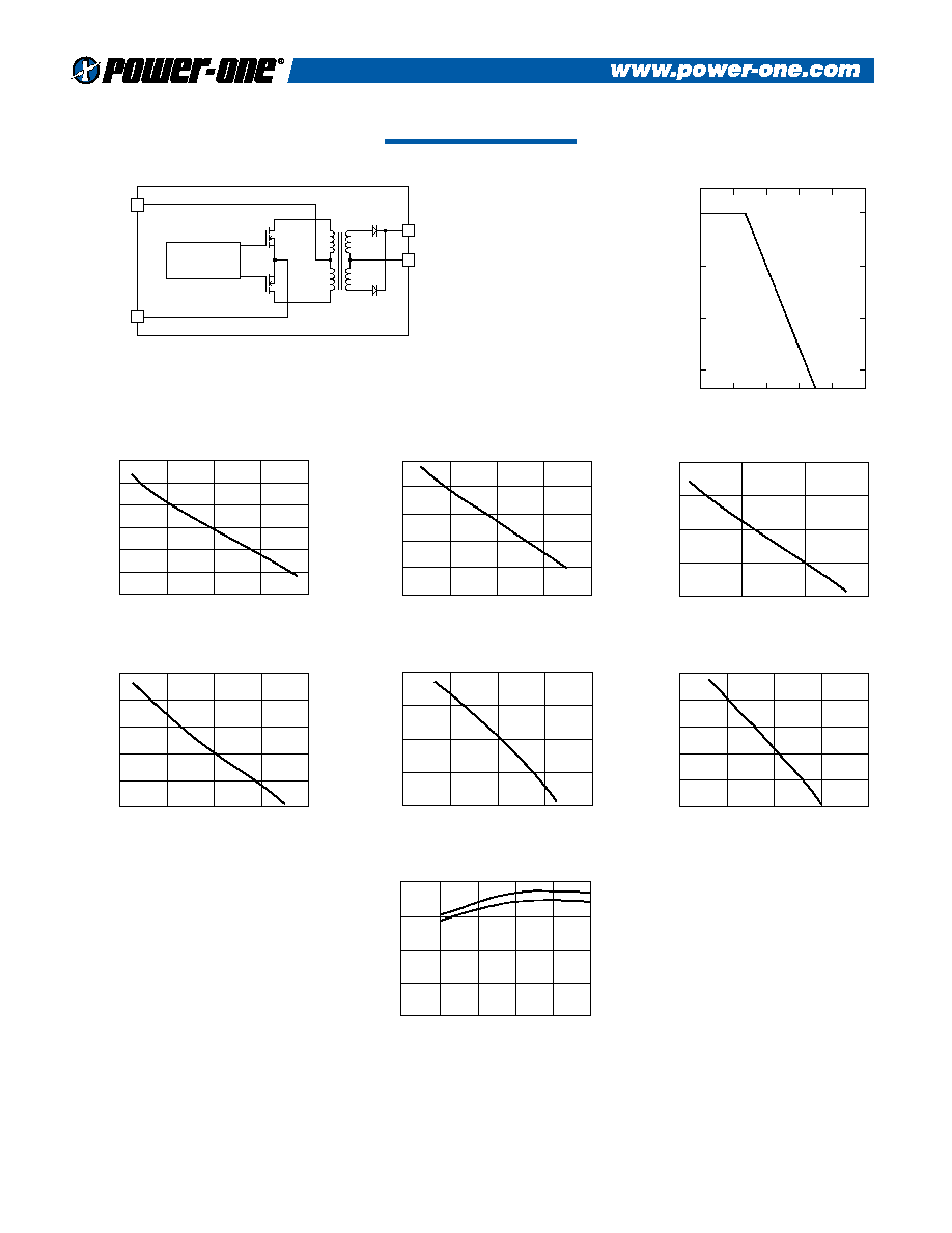
Typical Performance: (Tc=25∞C)
5.80
5.60
5.40
5.20
5.00
4.80
4.60
0
40
80
120
160
OUTPUT VOLTAGE Vs. OUTPUT LOAD
DSP1N5S5
OUTPUT LOAD (mA)
OUTPUT VOLTAGE (VOLTS)
13.50
13.00
12.50
12.00
11.50
0
30
60
90
OUTPUT VOLTAGE Vs. OUTPUT LOAD
DSP1N5S12
OUTPUT LOAD (mA)
OUTPUT VOLTAGE (VOLTS)
7.90
7.60
7.30
7.00
6.70
6.40
0
40
80
120
160
OUTPUT VOLTAGE Vs. OUTPUT LOAD
DSP1N5S7
OUTPUT LOAD (mA)
OUTPUT VOLTAGE (VOLTS)
15.40
15.00
14.20
14.60
13.80
13.40
0
20
40
60
80
OUTPUT VOLTAGE Vs. OUTPUT LOAD
DSP1N5S14
OUTPUT LOAD (mA)
OUTPUT VOLTAGE (VOLTS)
16.50
15.90
14.70
15.30
14.10
0
20
40
60
80
OUTPUT VOLTAGE Vs. OUTPUT LOAD
DSP1N5S15
OUTPUT LOAD (mA)
OUTPUT VOLTAGE (VOLTS)
18.50
18.00
17.00
16.50
17.50
16.00
0
20
40
60
80
OUTPUT VOLTAGE Vs. OUTPUT LOAD
DSP1N5S17
OUTPUT LOAD (mA)
OUTPUT VOLTAGE (VOLTS)
80
60
5-7 VOLT OUTPUT
12-17 VOLT OUTPUT
20
40
16
0
20
40
60
80
100
EFFICIENCY Vs. OUTPUT LOAD
% OF RATED LOAD (%)
EFFICIENCY (%)
DSP1 SERIES ≠ SINGLE OUPUT
1
2
4
+ OUTPUT
- OUT
+ INPUT
≠ INPUT
OSCILLATOR
DRIVER
3
DSP1 SERIES BLOCK DIAGRAM
50
0.4
0.6
0.8
1
60
70
80
90
100
OUTPUT POWER DERATING
AMBIENT TEMPERATURE
POWER OUTPUT
3