Sep. 2000
3.5
±
0.2 2.2
±
0.2DEPTH
85
±
0.2
+ 0
≠ 0.3
26
±
0.5
120MAX
(
127)
M3
!
0.5 2.5DEPTH
0.4MIN
0.4MIN
(6.8)
134
±
0.4
22.5
∞
±
0.5
∞
16-
4.5
+0.2
0
147
±
0.4
85
±
0.2
(4 )
A
A
A
kA
A
2
s
A/
µ
s
V
V
A
A
kW
kW
W
W
∞
C
∞
C
kN
g
MITSUBISHI GATE COMMUTATED TURN-OFF THYRISTORS
FGC3500AX-120DS
HIGH POWER INVERTER USE
PRESS PACK TYPE
FGC3500AX-120DS
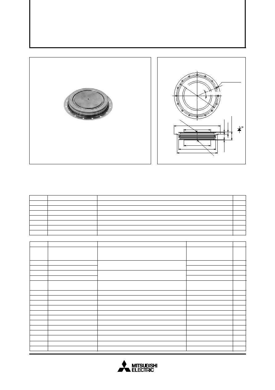
OUTLINE DRAWING
Dimensions in mm
3500
1800
1200
25
2.6
◊
10
6
1000
10
21
1000
3500
10
120
200
6300
≠20 ~ +125
≠20 ~ +150
32 ~ 48
1500
Repetitive controllable on-state current
RMS on-state current
Average on-state current
Surge on-state current
Current-squared, time integration
Critical rate of rise of on-state current
Peak forward gate voltage
Peak reverse gate voltage
Peak forward gate current
Peak reverse gate current
Peak forward gate power dissipation
Peak reverse gate power dissipation
Average forward gate power dissipation
Average reverse gate power dissipation
Junction temperature
Storage temperature
Mounting force required
Weight
APPLICATION
Inverters, DC choppers, Induction heaters, DC to DC converters.
Symbol
Parameter
Conditions
Ratings
Unit
+
: V
GK
= ≠2V
I
TQRM
I
T(RMS)
I
T(AV)
I
TSM
I
2t
d
iT
/d
t
V
FGM
V
RGM
I
FGM
I
RGM
P
FGM
P
RGM
P
FG(AV)
P
RG(AV)
T
j
T
stg
--
--
q
I
TQRM
Repetitive controllable on-state current .......... 3500A
q
I
T(AV)
Average on-state current .................... 1200A
q
V
DRM
Repetitive peak off-state voltage .................. 6000V
q
Anode short type
V
DM
= 6000V, V
D
= 3600V, L
C
= 0.3
µ
H, V
RG
= 20V
d
iGQ
/d
t
= 6000A/
µ
s, Tj = 25/125
∞
C
(see Fig. 1, 3)
Applied for all conduction angles
f = 60Hz, sinewave
= 180
∞
, T
f
= 70
∞
C
One half cycle at 60Hz, T
j
= 125
∞
C
V
D
= 3600V, I
T
= 3500A, I
GM
= 200A, T
j
= 125
∞
C
di
G
/d
t
= 100A/
µ
s
(see Fig. 1, 2)
(Recommended value 40kN)
Typical value
21
21
21
6000
6000
4800
3600
V
RRM
V
RSM
V
R(DC)
V
DRM
V
DSM
V
D(DC)
V
LTDS
Unit
Symbol
Parameter
V
V
V
V
V
V
V
Voltage class
Repetitive peak reverse voltage
Non-repetitive peak reverse voltage
DC reverse voltage
Repetitive peak off-state voltage
+
Non-repetitive peak off-state voltage
+
DC off-state voltage
+
Long term DC stability voltage
+
MAXIMUM RATINGS
PRELIMINARY
Notice: This is not a final specification.
Some parametric limits are subject to change.

Sep. 2000
--
--
--
--
--
--
--
--
V
TM
I
RRM
I
DRM
I
GRM
d
v
/d
t
I
GT
V
GT
R
th(j-f)
E
on
t
gt
V
D
d
V
/d
t
0.632V
D
/
0.632V
D
t
Rc
L(load)
FWDi
GCT
CDi
Cc
V
D
Lc
L(line)
GCT
L
V
D
V
D
t
gt
t
d
V
RG
I
GM
di
G
/d
t
t
s
I
G
V
RG
I
T
V
D
t
d
; 0V
G
~ 0.9V
D
t
gt
; 0V
G
~ 0.1V
D
di
G
/d
t
; 0.1I
GM
~ 0.9I
GM
t
s
; 0V
G
~ 0.9I
T
di
GQ
/d
t
; 0.1I
GQ
~ 0.9I
GQ
I
GQ
di
GQ/dt
On-state voltage
Repetitive peak reverse current
Repetitive peak off-state current
Reverse gate current
Critical rate of rise of off-state voltage
Gate trigger current
Gate trigger voltage
Thermal resistance
I
T
= 4000A, T
j
= 125
∞
C
V
RM
= 21V, T
j
= 125
∞
C
V
DM
= 6000V, V
GK
= ≠2V, T
j
= 125
∞
C
V
RG
= 21V, T
j
= 125
∞
C
V
D
= 3600V, V
GK
= ≠2V, T
j
= 125
∞
C
(Expo. wave)
(see Fig. 4)
V
D
= 3600V, I
T
= 3500A, d
i
/d
t
= 1000A/
µ
s
I
GM
= 200A, d
iG
/d
t
= 100A/
µ
s, T
j
= 125
∞
C
(see Fig. 1, 2)
V
DM
= 6000V, V
D
= 3600V, I
T
= 3500A
d
iGQ
/d
t
= 6000A/
µ
s, C
C
= 6
µ
F, L
C
= 0.3
µ
H
V
RG
= 20V, T
j
= 125
∞
C
(see Fig. 1, 3)
Junction to fin
MITSUBISHI GATE COMMUTATED TURN-OFF THYRISTORS
FGC3500AX-120DS
HIGH POWER INVERTER USE
PRESS PACK TYPE
ELECTRICAL CHARACTERISTICS
Symbol
Parameter
Test conditions
Limits
Min
Typ
Max
Unit
DC METHOD : V
D
= 24V, R
L
= 0.1
, T
j
= 25
∞
C
Fig. 1 Turn-on and Turn-off waveform
Fig. 2 Turn-on test circuit
Fig. 3 Turn-off test circuit
(With clamp circuit)
Fig. 4 dv/dt test waveform
Turn-on time
Turn-on switching energy
t
s
E
off
Storage time
Turn-off switching energy
3000
--
--
--
--
--
--
--
--
--
--
--
--
1.2
--
19
4.0
100
150
100
2.5
1.5
0.011
--
3.0
--
3.0
--
V
mA
mA
mA
A
V
∞
C/W
V/
µ
s
µ
s
J/P
µ
s
J/P
PRELIMINARY
Notice: This is not a final specification.
Some parametric limits are subject to change.
t
d
Delay time
--
--
1.0
µ
s

Sep. 2000
0
0.004
0.006
0.002
0.01
0.012
0.008
0.014
5
3
10
0
1
2
3
4
5
6
7
2
7
5
3
2
7
5
3
2
7
0
0
25
20
15
10
5
500 1000 1500 2000 2500 3000 3500 4000
2.0
0
1.8
1.6
1.4
1.2
1.0
0.8
0.6
0.4
0.2
0
4000
3500
3000
2500
2000
1500
1000
500
10
4
10
2
10
3
Tj=125
∞
C
Tj=25
∞
C
MAXIMUM ON-STATE CHARACTERISTIC
ON-STATE CURRENT
( A
)
ON-STATE VOLTAGE (V)
TURN ON SWITCHING ENERGY Eon (J/P)
TURN ON CURRENT (A)
TURN ON SWITCHING ENERGY
(TYPICAL)
TURN OFF SWITCHING ENERGY Eoff (J/P)
TURN OFF CURRENT (A)
TURN OFF SWITCHING ENERGY
(TYPICAL)
MAXIMUM THERMAL IMPEDANCE
CHARACTERISTIC
(JUNCTION TO FIN)
THERMAL IMPEDANCE Zth (
∞
C/W)
TIME (S)
Condition
V
D
=3600V, di/dt=1000A/
µ
s
I
GM
=200A, diG/dt=100A/
µ
s
Tj=125
∞
C
Condition
V
DM
=3600V+0.44
I
T
V
D
=3600V, C
C
=6
µ
F
L
C
=0.3
µ
F, Tj=125
∞
C
di
GQ
/dt=6000A/
µ
s
10
≠2
10
≠1
2 3 5 7
10
0
2 3 5 7
10
1
2 3 5 7
10
≠3
2 3 5 7
PERFORMANCE CURVES
MITSUBISHI GATE COMMUTATED TURN-OFF THYRISTORS
FGC3500AX-120DS
HIGH POWER INVERTER USE
PRESS PACK TYPE
PRELIMINARY
Notice: This is not a final specification.
Some parametric limits are subject to change.