Sep. 2001
PRELIMINARY
Notice: This is not a final specification.
Some parametric limits are subject to change.
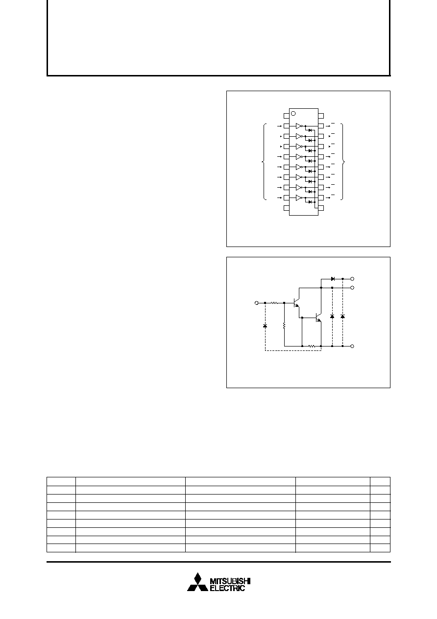
PIN CONFIGURATION
MITSUBISHI SEMICONDUCTOR <TRANSISTOR ARRAY>
M63820FP/KP
8-UNIT 500mA DARLINGTON TRANSISTOR-ARRAY WITH CLAMP DIODE
DESCRIPTION
The M63820FP/KP 8-channel sinkdriver, consists of 16 NPN
transistors connected to from eight high current gain driver
pairs.
FEATURES
G
High breakdown voltage (BV
CEO
50V)
G
High-current driving (I
C(max)
= 500mA)
G
With clamping diodes
G
3V micro computer series compatible input
G
Wide operating temperature range (Ta = ≠40 to +85
∞C)
APPLICATION
Output for 3 voltage microcomputer series and interface with
high voltage system. Relay and small printer driver, LED, or
incandescent display digit driver.
FUNCTION
The M63820FP/KP is transistor-array of high active level
eight units type which can do direct drive of 3 voltage micro-
computer series. A resistor of 1.05k
is connected between
the input pin. A clamp diode for inductive load transient sup-
pression is connected for the output pin (collector) and COM
pin (pin11). All emitters of the output transistor are con-
nected to GND (pin10). The outputs are capable of driving
500mA and are rated for operation with output voltage up to
50V.
1
2
3
4
5
6
7
8
9
10
20
19
18
17
16
15
14
13
12
11
NC
IN1
IN2
IN3
IN4
IN5
IN6
IN7
IN8
GND
NC
COM
COMMON
INPUT
OUTPUT
NC : No connection
O1
O2
O3
O4
O5
O6
O7
O8
Package type
20P2N-A(FP)
20P2E-A(KP)
CIRCUIT DIAGRAM
Unit :
COM
GND
1.05K
3K
7.2K
OUTPUT
INPUT
The eight circuits share the COM and GND
The diode, indicated with the dotted line, is parasitic, and
cannot be used.
Collector-emitter voltage
Collector current
Input voltage
Clamping diode forward current
Clamping diode reverse voltage
Power dissipation
Operating temperature
Storage temperature
V
mA
V
mA
V
W
∞C
∞C
≠0.5 ~ +50
500
≠0.5 ~ +10
500
50
1.10(GP)/0.68(KP)
≠40 ~ +85
≠55 ~ +125
Ratings
Symbol
Parameter
Conditions
Unit
ABSOLUTE MAXIMUM RATINGS
(Unless otherwise noted, Ta = ≠40 ~ +85
∞
C)
Output, H
Current per circuit output, L
Ta = 25
∞C, when mounted on board
V
CEO
I
C
V
I
I
F
V
R
P
d
T
opr
T
stg
POWEREX

Sep. 2001
PRELIMINARY
Notice: This is not a final specification.
Some parametric limits are subject to change.
MITSUBISHI SEMICONDUCTOR <TRANSISTOR ARRAY>
M63820FP/KP
8-UNIT 500mA DARLINGTON TRANSISTOR-ARRAY WITH CLAMP DIODE
--
--
I
C
400mA
Duty Cycle
FP : no more than 4%
KP : no more than 2%
RECOMMENDED OPERATING CONDITIONS
(Unless otherwise noted, Ta = ≠40 ~ +85
∞
C)
V
Parameter
0
Limits
min
typ
max
Symbol
Unit
V
O
Output voltage
"H" input voltage
"L" input voltage
Duty Cycle
FP : no more than 15%
KP : no more than 6%
Collector current (Current per
1 circuit when 8 circuits are
coming on simultaneously)
I
C
0
0
2.7
0
--
--
--
50
400
200
10
0.6
mA
V
V
V
IH
V
IL
TIMING DIAGRAM
NOTE 1 TEST CIRCUIT
ns
ns
--
--
15
350
--
--
Symbol
Unit
Parameter
Test conditions
Limits
min
typ
max
Turn-on time
Turn-off time
t
on
t
off
C
L
= 15pF (note 1)
SWITCHING CHARACTERISTICS
(Unless otherwise noted, Ta = 25
∞
C)
--
1.2
1.0
0.9
1.5
1.4
--
2500
50
--
--
--
--
--
--
1000
V
(BR) CEO
I
I
V
F
I
R
h
FE
V
V
mA
V
µA
--
--
1.6
1.3
1.1
2.4
2.0
100
--
Symbol
Unit
Parameter
Test conditions
Limits
min
typ
max
Collector-emitter breakdown voltage
Input current
Clamping diode forward volltage
Clamping diode reverse current
DC amplification factor
I
CEO
= 100
µA
I
I
= 500
µA, I
C
= 350mA
I
I
= 350
µA, I
C
= 200mA
I
I
= 250
µA, I
C
= 100mA
V
I
= 3V
I
F
= 350mA
V
R
= 50V
V
CE
= 2V, I
C
= 350mA
V
CE(sat)
Collector-emitter saturation voltage
ELECTRICAL CHARACTERISTICS
(Unless otherwise noted, Ta = 25
∞
C)
INPUT
50%
50%
50%
50%
OUTPUT
ton
toff
PG
INPUT
OUTPUT
V
O
R
L
OPEN
C
L
50
(1)Pulse generator (PG) characteristics : PRR=1kHz,
tw = 10
µs, tr = 6ns, tf = 6ns, Zo = 50
V
I
= 0 ~ 3V
(2)Input-output conditions : R
L
= 25
, Vo = 10V
(3)Electrostatic capacity C
L
includes floating capacitance
at connections and input capacitance at probes
Measured device
POWEREX