 | –≠–ª–µ–∫—Ç—Ä–æ–Ω–Ω—ã–π –∫–æ–º–ø–æ–Ω–µ–Ω—Ç: M63830P | –°–∫–∞—á–∞—Ç—å:  PDF PDF  ZIP ZIP |
Sep. 2001
PRELIMINARY
Notice: This is not a final specification.
Some parametric limits are subject to change.
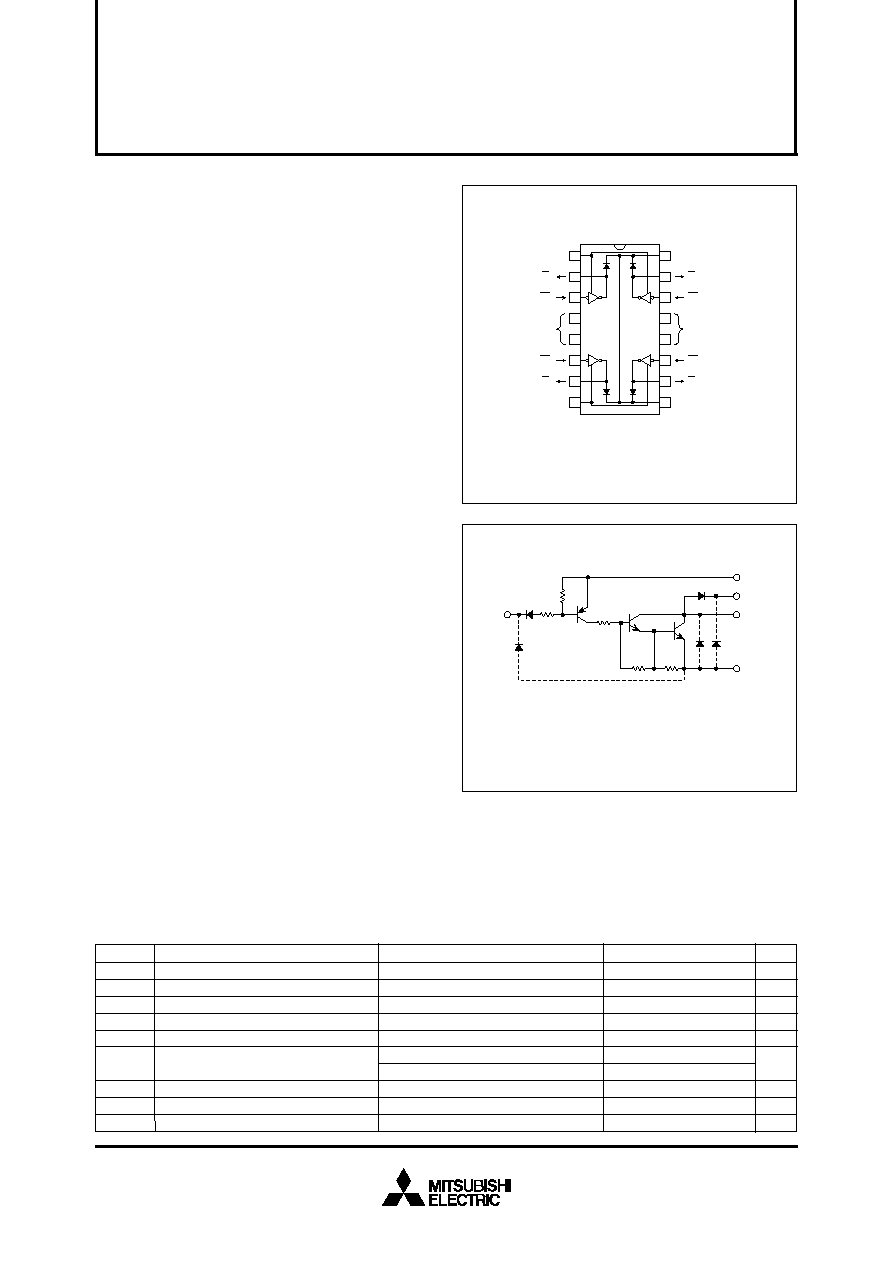
PIN CONFIGURATION
MITSUBISHI SEMICONDUCTOR <TRANSISTOR ARRAY>
M63830P/FP
4-UNIT 1.5A DARLINGTON TRANSISTOR-ARRAY WITH CLAMP DIODE
DESCRIPTION
The M63830P/FP 4-channel sinkdriver, consists of 4 PNP
and 8 NPN transistors connected to from four high current
gain driver pairs.
FEATURES
G
High breakdown voltage (BV
CEO
50V)
G
High-current driving (I
C(max)
= 1.5A)
G
3V micro computer series compatible input
G
With clamping diodes
G
With input diode
G
Wide operating temperature range (Ta = ≠40 to +85
∞C)
APPLICATION
Output for 3 voltage microcomputer series and interface with
high voltage system. Relay and small printer driver, LED, or
incandescent display digit driver.
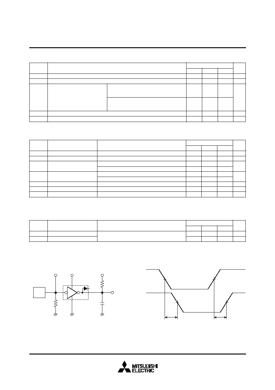
FUNCTION
The M63830FP/P is transistor-array of high active level four
units type which can do direct drive of 3 voltage microcom-
puter series. A resistor of 3.5k
is connected between the
input and the base of PNP transistors. A clamp diode for in-
ductive load transient suppression is connected for the out-
put pin (collector) and COM pin. The input diode is intended
to prevent the flow of current from the input to the Vcc. With-
out this diode, the current flows from "H" input to the Vcc and
the "L" input circuit is activated, in such a case where one of
the inputs of the 4 circuit is "H" and the other are "L" to save
power consumption. The diode is inserted to prevent such
mis-operation. The outputs are capable of driving 1.5A and
are rated for operation with output voltage up to 50V.
Supply voltage
Collector-emitter voltage
Collector current
Input voltage
Clamping diode reverse voltage
Clamping diode forward current
Power dissipation
Operating temperature
Storage temperature
V
V
A
V
V
A
W
∞C
∞C
7
≠0.5 ~ +50
1.5
≠0.5 ~ V
CC
50
1.5
1.0
1.92(P)/1.00(FP)
≠40 ~ +85
≠55 ~ +125
Ratings
Symbol
Parameter
Conditions
Unit
ABSOLUTE MAXIMUM RATINGS
(Unless otherwise noted, Ta = ≠40 ~ +85
∞
C)
Output, H
Current per circuit output, L
Pulse width
10ms, duty cycle 5%
Pulse width
100ms, duty cycle 5%
Ta = 25
∞C, when mounted on board
V
CC
V
CEO
I
C
V
I
V
R
I
F
P
d
T
opr
T
stg
CIRCUIT DIAGRAM
INPUT
3.5K
5.5K
3K
760
22K
V
CC
COM
GND
OUTPUT
Unit :
The four circuits share the COM and GND
The diode, indicated with the dotted line, is parasitic, and
cannot be used.
1
2
3
4
5
6
7
8
16
15
14
13
12
11
10
9
V
CC
V
CC
GND
O1
IN1
OUTPUT1
O2
OUTPUT2
INPUT1
IN2
INPUT2
COM COMMON
COM COMMON
GND
O4
IN4
OUTPUT4
INPUT4
O3
IN3
OUTPUT3
INPUT3
Package type
16P4(P)
16P2N-A(FP)
POWEREX
Sep. 2001
PRELIMINARY
Notice: This is not a final specification.
Some parametric limits are subject to change.
MITSUBISHI SEMICONDUCTOR <TRANSISTOR ARRAY>
M63830P/FP
4-UNIT 1.5A DARLINGTON TRANSISTOR-ARRAY WITH CLAMP DIODE
--
--
RECOMMENDED OPERATING CONDITIONS
(Unless otherwise noted, Ta = ≠40 ~ +85
∞
C)
V
V
Parameter
2.7
0
Limits
min
typ
max
Symbol
Unit
V
CC
V
O
Supply voltage
Output voltage
"H" input voltage
"L" input voltage
Collector current (Current per
1 circuit when 4 circuits are
coming on simultaneously)
I
C
0
0
V
CC
-0.5
0
3.0
--
--
--
3.6
50
1.25
0.7
V
CC
V
CC
-2.2
A
V
V
V
IH
V
IL
V
CC
= 3V, Duty Cycle
P : no more than 5%
FP : no more than 2%
V
CC
= 3V, Duty Cycle
P : no more than 15%
FP : no more than 7%
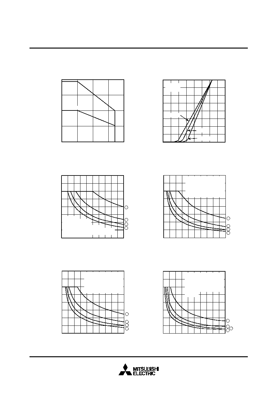
TIMING DIAGRAM
NOTE 1 TEST CIRCUIT
INPUT
50%
50%
50%
50%
OUTPUT
ton
toff
PG
INPUT
V
CC
OUTPUT
V
O
R
L
OPEN
C
L
50
(1)Pulse generator (PG) characteristics : PRR=1kHz,
tw = 10
µs, tr = 6ns, tf = 6ns, Zo = 50
V
I
= 0.5 ~ 2.7V
(2)Input-output conditions : R
L
= 8.3
, Vo = 10V, Vcc = 2.7V
(3)Electrostatic capacity C
L
includes floating capacitance
at connections and input capacitance at probes
Measured
device
ns
ns
--
--
190
5300
--
--
Symbol
Unit
Parameter
Test conditions
Limits
min
typ
max
Turn-on time
Turn-off time
t
on
t
off
C
L
= 15pF (note 1)
SWITCHING CHARACTERISTICS
(Unless otherwise noted, Ta = 25
∞
C)
--
3.7
1.4
1.0
≠0.22
≠0.60
--
1.5
30000
50
--
--
--
--
--
--
--
4000
V
(BR) CEO
I
CC
I
I
I
R
V
F
h
FE
V
mA
V
mA
µA
V
--
--
5.0
2.2
1.7
≠0.6
≠0.95
100
2.3
--
Symbol
Unit
Parameter
Test conditions
Limits
min
typ
max
Collector-emitter breakdown voltage
Supply current (AN only Input)
Input current
Clamping diode reverse current
Clamping diode forward volltage
DC amplification factor
I
CEO
= 100
µA
V
CC
= 3.6V, V
I
= 0.5V
V
CC
= 2.7V, V
I
= 0.5V, I
C
= 1.25A
V
CC
= 2.7V, V
I
= 0.5V, I
C
= 0.7A
V
I
= V
CC
-2.2V
V
I
= V
CC
-3.6V
V
R
= 50V
I
F
= 1.25A, V
CC
open
V
CC
= 2.7V, V
CE
= 2V, I
C
= 1A, Ta = 25
∞C
V
CE(sat)
Collector-emitter saturation voltage
ELECTRICAL CHARACTERISTICS
(Unless otherwise noted, Ta = ≠40 ~ +85
∞
C)
: Typical values are at Ta = 25∞C
POWEREX
Sep. 2001
PRELIMINARY
Notice: This is not a final specification.
Some parametric limits are subject to change.
MITSUBISHI SEMICONDUCTOR <TRANSISTOR ARRAY>
M63830P/FP
4-UNIT 1.5A DARLINGTON TRANSISTOR-ARRAY WITH CLAMP DIODE
TYPICAL CHARACTERISTICS
1.2
0.8
0.4
0
0
0.5
1.0
1.5
2.0
1.6
Ta=≠40
∞C
Ta=25
∞C
Ta=85
∞C
Vcc=2.7V
V
I
=0.5V
Collector current Ic (A)
Output saturation voltage V
CE(sat)
(V)
M63830P
M63830FP
0.520
0.998
0
25
50
75 85
100
0
1.0
0.5
1.5
2.0
1.92
Thermal Derating Factor Characteristics
Ambient temperature Ta (
∞C)
Power dissipation Pd(max) (W)
Output Saturation Voltage
Collector Current Characteristics
Duty Cycle-Collector Characteristics
(M63830P)
0
1.0
0.5
1.5
2.0
0
20
40
60
80
100
Duty cycle (%)
Collector current Ic (A)
∑The collector
current values represent
the current per circuit.
∑Repeated frequency
10Hz
∑The value the circle represents the
value of the simultaneously-operated circuit.
∑Vcc = 3V ∑Ta = 25
∞C
1
2
3
4
Duty Cycle-Collector Characteristics
(M63830P)
0
1.0
0.5
1.5
2.0
Collector current Ic (A)
0
20
40
60
80
100
Duty cycle (%)
∑The collector current values
represent the current per circuit.
∑Repeated frequency
10Hz
∑The value the circle represents
the value of the simultaneously-
operated circuit.
∑Vcc = 3V ∑Ta = 85
∞C
1
2
3
4
Duty Cycle-Collector Characteristics
(M63830FP)
0
1.0
0.5
1.5
2.0
0
20
40
60
80
100
Duty cycle (%)
Collector current Ic (A)
1
2
3
4
∑The collector current values
represent the current per circuit.
∑Repeated frequency
10Hz
∑The value the circle represents
the value of the
simultaneously-operated circuit.
∑Vcc = 3V ∑Ta = 25
∞C
0
1.0
0.5
1.5
2.0
0
20
40
60
80
100
Duty cycle (%)
Collector current Ic (A)
Duty Cycle-Collector Characteristics
(M63830FP)
∑The collector current values
represent the current per circuit.
∑Repeated frequency
10Hz
∑The value the circle represents
the value of the
simultaneously-operated circuit.
∑Vcc = 3V
∑Ta = 85
∞C
1
2
3
4
POWEREX

Sep. 2001
PRELIMINARY
Notice: This is not a final specification.
Some parametric limits are subject to change.
MITSUBISHI SEMICONDUCTOR <TRANSISTOR ARRAY>
M63830P/FP
4-UNIT 1.5A DARLINGTON TRANSISTOR-ARRAY WITH CLAMP DIODE
Ta=≠40
∞C
Ta=25
∞C
DC Amplification Factor
Collector Current Characteristics
Ta=85
∞C
Collector current I
C
(mA)
DC amplification f
actor h
FE
10
2
10
3
3
2
5
7
10
4
10
5
3
2
5
7
3
2
5
7
10
2
3
2
5 7
10
3
3
2
5 7
10
4
10
1
3
2
5 7
V
CC
=2.7V
V
CE
=2V
Collector current Ic (A)
0
0.5
1.0
1.5
2.0
Input voltage Vcc-V
I
(V)
Grounded Emitter Transfer Characteristics
0
0.8
0.4
1.2
1.6
V
CC
=2.7V
V
CE
=2V
Ta=85
∞C
Ta=25
∞C
Ta=≠40
∞C
Input Characteristics
V
CC
=3V
Ta=≠20
∞C
Ta=25
∞C
Ta=85
∞C
Input Current I
I
(mA)
0
1
2
3
Input voltage Vcc-V
I
(V)
0
≠0.3
≠0.2
≠0.1
≠0.4
≠0.5
≠0.6
Clamping Diode Characteristics
F
orw
ard bias current I
F
(A)
0
0.5
1.0
1.5
2.0
Forward bias voltage V
F
(V)
0
1.0
0.5
1.5
2.0
Ta=25
∞C
Ta=85
∞C
Ta=≠40
∞C
Driver Supply Characteristics
Supply Current Icc (mA)
0
2
4
6
8
10
Supply voltage Vcc (V)
0
8.0
4.0
12.0
16.0
20.0
V
I
=0.5V
Ta=25
∞C
Ta=≠40
∞C
Ta=85
∞C
POWEREX