 | –≠–ª–µ–∫—Ç—Ä–æ–Ω–Ω—ã–π –∫–æ–º–ø–æ–Ω–µ–Ω—Ç: M63836KP | –°–∫–∞—á–∞—Ç—å:  PDF PDF  ZIP ZIP |
Sep. 2001
PRELIMINARY
Notice: This is not a final specification.
Some parametric limits are subject to change.
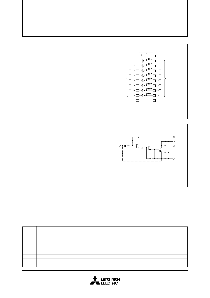
PIN CONFIGURATION
MITSUBISHI SEMICONDUCTOR <TRANSISTOR ARRAY>
M63836FP/KP
8-UNIT 500mA DARLINGTON TRANSISTOR-ARRAY WITH CLAMP DIODE
DESCRIPTION
The M63836FP/KP 8-channel sinkdriver, consists of 8 PNP
and 16 NPN transistors connected to from eight high current
gain driver pairs.
FEATURES
G
High breakdown voltage (BV
CEO
50V)
G
High-current driving (I
C(max)
= 500mA)
G
3V micro computer compatible input
G
"L" active level input
G
With input diode
G
With clamping diodes
G
Wide operating temperature range (Ta = ≠40 to +85
∞C)
APPLICATION
Output for 3 voltage microcomputer series and interface with
high voltage system. Relay and small printer driver, LED, or
incandescent display digit driver.
FUNCTION
The M63836FP/KP is transistor-array of high active level
eight units type which can do direct drive of 3 voltage micro-
computer series. A resistor of 3.5k
is connected between
the input and the base of PNP transistors. A clamp diode for
inductive load transient suppression is connected for the
output pin (collector) and COM pin. The input diode is in-
tended to prevent the flow of current from the input to the
Vcc. without this diode, the current flows from "H" input to the
Vcc and the "L" input circuit is activated, in such a case
where one of the inputs of the 8 circuit is "H" and the other
are "L" to save power consumption. The diode is inserted to
prevent such mis-operation. The outputs are capable of driv-
ing 500mA and are rated for operation with output voltage up
to 50V.
CIRCUIT DIAGRAM
INPUT
3.5K
7.2K
3K
1.05K
20K
V
CC
COM
GND
OUTPUT
Unit :
The eight circuits share the Vcc, COM and GND
The diode, indicated with the dotted line, is parasitic, and
cannot be used.
Supply voltage
Collector-emitter voltage
Collector current
Input voltage
Clamping diode forward current
Clamping diode reverse voltage
Power dissipation
Operating temperature
Storage temperature
V
V
mA
V
mA
V
W
∞C
∞C
7
≠0.5 ~ +50
500
≠0.5 ~ V
CC
500
50
1.10(FP)/0.68(KP)
≠40 ~ +85
≠55 ~ +125
Ratings
Symbol
Parameter
Conditions
Unit
ABSOLUTE MAXIMUM RATINGS
(Unless otherwise noted, Ta = ≠40 ~ +85
∞
C)
Output, H
Current per circuit output, L
Ta = 25
∞C, when mounted on board
V
CC
V
CEO
I
C
V
I
I
F
V
R
P
d
T
opr
T
stg
1
2
3
4
5
6
7
8
9
10
20
19
18
17
16
15
14
13
12
11
NC
IN1
GND
COM COMMON
V
CC
INPUT
OUTPUT
O1
O2
O3
O4
O5
O6
O7
O8
IN2
IN3
IN4
IN5
IN6
IN7
IN8
NC : No connection
Package type
20P2N-A(FP)
20P2E-A(KP)
POWEREX
Sep. 2001
PRELIMINARY
Notice: This is not a final specification.
Some parametric limits are subject to change.
MITSUBISHI SEMICONDUCTOR <TRANSISTOR ARRAY>
M63836FP/KP
8-UNIT 500mA DARLINGTON TRANSISTOR-ARRAY WITH CLAMP DIODE
--
--
RECOMMENDED OPERATING CONDITIONS
(Unless otherwise noted, Ta = ≠40 ~ +85
∞
C)
V
Parameter
2.7
Limits
min
typ
max
Symbol
Unit
V
CC
Supply voltage
"H" input voltage
"L" input voltage
Collector current (Current per
1 circuit when 8 circuits are
coming on simultaneously)
I
C
0
0
V
CC
-0.5
0
3.0
--
--
3.6
400
200
V
CC
V
CC
-2.2
mA
V
V
V
IH
V
IL
Duty Cycle
FP : no more than 4%
KP : no more than 2%
Duty Cycle
FP : no more than 15%
KP : no more than 6%
ELECTRICAL CHARACTERISTICS
(Unless otherwise noted, Ta = ≠40 ~ +85
∞
C)
: Typical values are at Ta = 25∞C
--
1.15
0.93
≠220
1.4
0.1
2.6
10000
50
--
--
--
--
--
--
2000
V
(BR) CEO
I
I
V
F
I
R
I
CC
h
FE
V
V
µA
V
µA
mA
--
--
2.4
1.6
≠600
2.4
100
4.0
--
Symbol
Unit
Parameter
Test conditions
Limits
min
typ
max
Collector-emitter breakdown voltage
Input current
Clamping diode forward volltage
Clamping diode reverse current
Supply current (AN only Input)
DC amplification factor
I
CEO
= 100
µA
V
CC
= 2.7V, V
I
= 0.5V, I
C
= 400mA
V
CC
= 2.7V, V
I
= 0.5V, I
C
= 200mA
V
I
= V
CC
-2.2V
I
F
= 400mA
V
R
= 50V
V
CC
= 3.6V, V
I
= 0.5V
V
CC
= 2.7V, V
CE
= 2V, I
C
= 0.35A, Ta = 25
∞C
V
CE(sat)
Collector-emitter saturation voltage
ns
ns
--
--
120
4500
--
--
Symbol
Unit
Parameter
Test conditions
Limits
min
typ
max
Turn-on time
Turn-off time
t
on
t
off
C
L
= 15pF (note 1)
SWITCHING CHARACTERISTICS
(Unless otherwise noted, Ta = 25
∞
C)
TIMING DIAGRAM
NOTE 1 TEST CIRCUIT
INPUT
50%
50%
50%
50%
OUTPUT
ton
toff
PG
INPUT
V
CC
OUTPUT
V
O
R
L
OPEN
C
L
50
(1)Pulse generator (PG) characteristics : PRR=1kHz,
tw = 10
µs, tr = 6ns, tf = 6ns, Zo = 50
V
I
= 0.5 ~ 2.7V
(2)Input-output conditions : R
L
= 30
, Vo = 10V, Vcc = 2.7V
(3)Electrostatic capacity C
L
includes floating capacitance
at connections and input capacitance at probes
Measured
device
POWEREX

Sep. 2001
PRELIMINARY
Notice: This is not a final specification.
Some parametric limits are subject to change.
MITSUBISHI SEMICONDUCTOR <TRANSISTOR ARRAY>
M63836FP/KP
8-UNIT 500mA DARLINGTON TRANSISTOR-ARRAY WITH CLAMP DIODE
TYPICAL CHARACTERISTICS
Thermal Derating Factor Characteristics
2.0
1.5
1.0
0.5
0
0
25
50
75
100
M63836KP
M63836FP
85
0.572
0.354
1.10
0.68
Power dissipation Pd(max) (W)
Ambient temperature Ta (
∞C)
Output Saturation Voltage
Collector Current Characteristics
400
300
200
100
0
0
0.5
1.0
1.5
2.0
500
Collector current Ic (mA)
Output saturation voltage V
CE(sat)
(V)
Vcc=2.7V
V
I
=0.5V
Ta= 85
∞C
Ta= 25
∞C
Ta= ≠20
∞C
500
400
300
200
100
0
0
100
20
40
60
80
Duty cycle (%)
Collector current Ic (mA)
500
400
300
200
100
0
100
20
40
60
80
0
Duty cycle (%)
Collector current Ic (mA)
500
400
300
200
100
0
100
20
40
60
80
0
Duty cycle (%)
Collector current Ic (mA)
Duty Cycle-Collector Characteristics
(M63836FP)
Duty Cycle-Collector Characteristics
(M63836GFP)
Duty Cycle-Collector Characteristics
(M63836KP)
500
400
300
200
100
0
100
20
40
60
80
0
Duty cycle (%)
Duty Cycle-Collector Characteristics
(M63836KP)
Collector current Ic (mA)
∑The collector
current values
represent the current per circuit.
∑Repeated frequency
10Hz
∑The value the circle represents the
value of the simultaneously-operated circuit.
∑Vcc = 3V ∑Ta = 25
∞C
1
2
7
3
4
5
8
6
1
2
7
5
3
4
8
6
1
2
7
5
3
4
8
6
1
2
7
5
3
4
8
6
∑The collector current values
represent the current per circuit.
∑Repeated frequency
10Hz
∑The value the circle
represents the value
of the simultaneously-
operated circuit.
∑Vcc = 3V
∑Ta = 85
∞C
∑The collector
current values
represent the
current per circuit.
∑Repeated frequency
10Hz
∑The value the circle represents the value of the
simultaneously-operated circuit. ∑Vcc = 3V ∑Ta = 85
∞C
∑The collector
current values
represent the
current per circuit.
∑Repeated frequency
10Hz
∑The value the circle represents the value of the
simultaneously-operated circuit. ∑Vcc = 3V ∑Ta = 25
∞C
POWEREX

Sep. 2001
PRELIMINARY
Notice: This is not a final specification.
Some parametric limits are subject to change.
MITSUBISHI SEMICONDUCTOR <TRANSISTOR ARRAY>
M63836FP/KP
8-UNIT 500mA DARLINGTON TRANSISTOR-ARRAY WITH CLAMP DIODE
DC Amplification Factor
Collector Current Characteristics
Collector current I
C
(mA)
DC amplification f
actor h
FE
10
2
10
3
3
2
5
7
10
4
3
2
5
7
10
5
3
2
5
7
10
2
3
2
5 7
10
3
3
2
5 7
10
1
V
CE
=2V
Ta=85
∞C
Ta=25
∞C
Ta=≠40
∞C
Collector current I
C
(mA)
0
0.4
0.8
1.2
2.0
1.6
Input voltage Vcc-V
I
(V)
Output Current Characteristics
0
200
100
300
400
500
V
CE
=2V
Ta=85
∞C
Ta=25
∞C
Ta=≠40
∞C
Input Characteristics
Input Current I
I
(mA)
1
0
2
3
Input voltage Vcc-V
I
(V)
0
≠0.3
≠0.2
≠0.1
≠0.4
≠0.5
≠0.6
V
CC
=3V
Ta=85
∞C
Ta=25
∞C
Ta=≠40
∞C
Driver Supply Characteristics
Supply Current Icc (mA)
0
2
4
6
8
10
Supply voltage Vcc (V)
0
8.0
4.0
12.0
16.0
20.0
Ta=25
∞C
Ta=85
∞C
Ta=≠40
∞C
V
I
=0.5V
Clamping Diode Characteristics
F
orw
ard bias current I
F
(mA)
0
0.5
1.0
1.5
2.0
Forward bias voltage V
F
(V)
0
Ta=≠40
∞C
Ta=25
∞C
Ta=85
∞C
300
200
100
400
500
POWEREX