 | –≠–ª–µ–∫—Ç—Ä–æ–Ω–Ω—ã–π –∫–æ–º–ø–æ–Ω–µ–Ω—Ç: PS11011 | –°–∫–∞—á–∞—Ç—å:  PDF PDF  ZIP ZIP |

MITSUBISHI SEMICONDUCTOR <Application Specific Intelligent Power Module>
PS11011
FLAT-BASE TYPE
INSULATED TYPE
Jan. 2000
PS11011
INTEGRATED FUNCTIONS AND FEATURES
∑ Converter bridge for 3 phase AC-to-DC power conversion.
∑ Circuit for dynamic braking of motor regenerative energy.
∑ 3-phase IGBT inver ter bridge configured by the latest 3rd.
generation IGBT and diode technology.
∑ Inverter output current capability I
O
(Note 1):
APPLICATION
Acoustic noise-less 0.1kW/AC200V class 3 phase inverter and other motor control applica-
tions
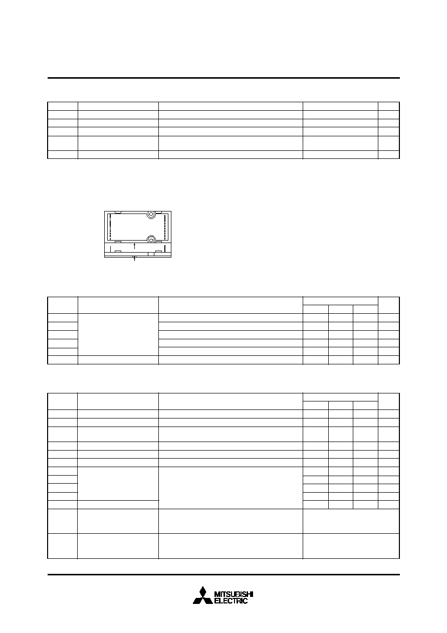
PACKAGE OUTLINES
MITSUBISHI SEMICONDUCTOR <Application Specific Intelligent Power Module>
PS11011
FLAT-BASE TYPE
INSULATED TYPE
INTEGRATED DRIVE, PROTECTION AND SYSTEM CONTROL FUNCTIONS:
∑ For inverter side upper-leg IGBTs : Drive circuit, High voltage isolated high-speed level shifting, Short circuit protection (SC).
Bootstrap circuit supply scheme (single drive power supply) and Under voltage protection (UV).
∑ For inverter side lower-leg IGBTs : Drive circuit, Short circuit protection (SC).
Control supply circuit under- & over- voltage protection (OV/UV).
System over temperature protection (OT). Fault output signaling circuit (F
O
) and Current limit warn-
ing signal output (CL).
∑ For Brake circuit IGBT : Drive circuit
∑ Warning and Fault signaling :
F
O1
: Short circuit protection for lower-leg IGBTs and Input interlocking against spurious arm shoot-through.
F
O2
: N-side control supply abnormality locking (OV/UV).
F
O3
: System over-temperature protection (OT).
CL : Warning for inverter current overload condition
∑ For system feedback control : Analogue signal feedback reproducing actual inverter output phase currents (3
).
∑ Input Interface : 5V CMOS/TTL compatible, Schmitt trigger input, and Arm-Shoot-Through interlock protection.
(Note 1) : The inverter output current is assumed to be sinu-
soidal and the peak current value of each of the
above loading cases is defined as : I
OP
= I
O
◊
2
(Fig. 1)
Type Name
PS11011
100% load
0.8A (rms)
150% over load
1.2A (rms), 1min
1 CBU+
2 CBU≠
3 CBV+
4 CBV≠
5 CBW+
6 CBW≠
7 GND
8 NC
9 VDH
10 CL
11 FO1
12 FO2
13 FO3
14 CU
15 CV
16 CW
17 UP
18 VP
19 WP
20 UN
21 VN
22 WN
23 Br
31 R
32 S
33 T
34 P1
35 P2
36 N
37 B
38 U
39 V
40 W
2
±
0.3
54
±
0.5
0.5
±
0.03
0.8
0~0.8
0~0.8
0.4
0.5
62
±
1
20.4
±
1
27
±
1
84.2
±
1
72
±
0.8
17.6
±
0.5
5.08
±
0.3
!
9 = 45.72
±
0.8
4-R2
2-R4
0.5
2
2
4.14
4
0.5
4
24
0.6
8.5
12
(12.25)
50
6
2
2 4
4
4
1 2 3 4
5 6
7 8 9101112131415161718192021 23
31
32
33
34
35
36
37
38
39
40
22
Terminals Assignment:
2-
4
1.2
LABEL
3.5
V
V
V
V
Control Pin top
portion details
V
Main terminal top
portion details
0.3
±
0.5
0
12
0.6
0.35MAX
±
0.5
0
MITSUBISHI SEMICONDUCTOR <Application Specific Intelligent Power Module>
PS11011
FLAT-BASE TYPE
INSULATED TYPE
Jan. 2000
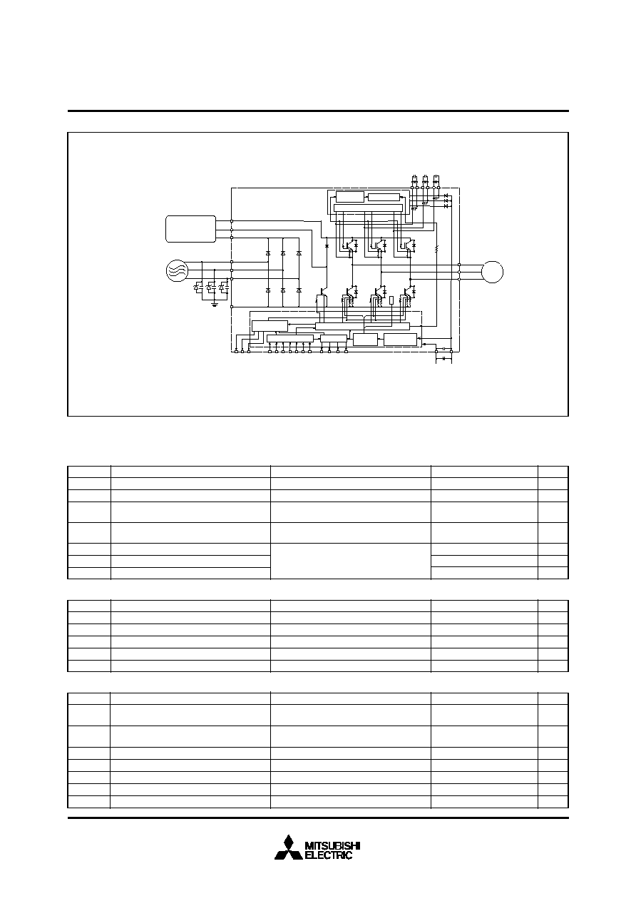
(15V line)
VDH
GND
CUCV CW
U
P
V
P
W
P
U
N
V
N
W
N
B
r
CL FO1 FO2 FO3
B
P2
P1
R
S
T
C
Z
N
M
W
V
U
AC200V line input
C3 ; 3.3
µ
F or more, tight tolerance, temp-compensated electrolytic type (Note : the value may change
depending on the type PWM control scheme used in the applied system)
C4 ; 2
µ
F R-category ceramic condenser for noise filtering.
C2 ;
3.3
µ
F or more
FO Logic
Protection
Circuit
Level shifter
Drive Circuit
Drive Curcuit
Trig signal conditioning
Current sensing
circuit
Protection
circuit
Control supply
fault sense
Z : Surge absorber.
C : AC filter (Ceramic condenser 2.2~6.5nF)
[Note : Additionally an appropriate Line-to line
surge absorber circuit maybe necessary
depending on the application environment].
AC 200V line
output
Brake resistor
connection,
Inrush prevention
circuit, etc.
Note 1) To prevent chances of signal oscillation, an RC coupling at each output is recommended. (see also Fig.10)
Note 2) By virtue of integrating an application specific type HVIC inside the module, direct coupling to CPU, without any opto or transformer isolation ispossible. (see also Fig.10)
Note 3) All these outputs are open collector type. Each signal line should be pulled up to plus side of the 5V power supply with approximately 5.1k
resistance. (see also Fig.10)
Note 4) The wiring between power DC link capacitor and P/N terminals should be as short as possible to protect the ASIPM against catastrophic high surge voltage. For extra
precaution, a small film type snubber capacitor (0.1~0.22
µ
F, high voltage type) is recommended to be mounted close to these P and N DC powerinput pins.
Analogue signal output corresponding to
each phase current (5V line) Note 1)
Each phase input (PWM)
(5V line) Note 2)
Fault output
(5V line) Note 3)
CBU≠
CBU+
CBV≠
CBV+
CBW≠
CBW+
C4,C3
Application Specific Intelligent
Power Module
T.S.
C2
Each output IGBT collector current
Brake IGBT collector current
Brake diode anode current
INTERNAL FUNCTIONS BLOCK DIAGRAM
(Fig. 2)
V
V
450
500
Applied between P2-N
Applied between P2-N, Surge-value
Applied between P-U, V, W, Br or U, V, W,
Br-N
Applied between P-U, V, W, Br or U, V, W,
Br-N
T
C
= 25
∞
C
Note: "( )" means I
C
peak value
Supply voltage
Supply voltage (surge)
V
CC
V
CC(surge)
Condition
Symbol
Item
Ratings
Unit
MAXIMUM RATINGS
(Tj = 25
∞
C)
INVERTER PART (Including Brake Part)
V
P
or V
N
V
P(S)
or V
N(S)
±
I
C
(
±
I
CP
)
I
C
(I
CP
)
I
F
(I
FP
)
Each output IGBT collector-emitter static voltage
Each output IGBT collector-emitter
switching surge voltage
600
600
±
2 (
±
4)
2 (4)
2 (4)
V
V
A
A
A
V
20
Fault output supply voltage
Fault output current
Current-limit warning (CL) output voltage
CL output current
Analogue current signal output current
Applied between V
DH
-GND, C
BU+
-C
BU≠
,
C
BV+
-C
BV≠
, C
BW+
-C
BW≠
Applied between U
P
∑ V
P
∑ W
P
∑ U
N
∑ V
N
∑
W
N
∑ B
r
-GND
Applied between F
O1
∑ F
O2
∑ F
O3
-GND
Sink current of F
O1
∑ F
O2
∑ F
O3
Applied between CL-GND
Sink current of CL
Sink current of CU ∑ CV ∑ CW
V
DH
, V
DB
Supply voltage
Symbol
Item
Ratings
Unit
CONTROL PART
Condition
V
FO
I
FO
V
CL
I
CL
I
CO
V
CIN
Input signal voltage
≠0.5 ~ 7.5
≠0.5 ~ 7
15
≠0.5 ~ 7
15
±
1
V
V
mA
V
mA
mA
3
rectifying circuit
1 cycle at 60Hz, peak value non-repetitive
Value for one cycle of surge current
Condition
Symbol
Item
Ratings
Unit
V
RRM
Ea
I
O
I
FSM
I
2
t
Repetitive peak reverse voltage
Recommended AC input voltage
DC output current
Surge (non-repetitive) forward current
I
2
t for fusing
800
220
25
138
80
V
V
A
A
A
2
s
CONVERTER PART
MITSUBISHI SEMICONDUCTOR <Application Specific Intelligent Power Module>
PS11011
FLAT-BASE TYPE
INSULATED TYPE
Jan. 2000
--
0.1
V
CC
400V, Input = ON (one-shot)
Tj = 125
∞
C start
13.5V
V
DH
= V
DB
16.5V
V
CC
400V, Tj
125
∞
C,
Ic < I
OL
(CL) operation level, Input = ON
13.5V
V
DH
= V
DB
16.5V
V
V
--
V
FBr
I
RRM
V
FR
ton
tc(on)
toff
tc(off)
trr
TC
7.3
6.1
7.3
6.1
4.8
0.053
Collector-emitter saturation voltage
FWDi forward voltage
Brake IGBT
Collector-emitter saturation voltage
Brake diode forward voltage
Converter diode reverse current
Converter diode voltage
Switching times
FWD reverse recovery time
V
CE(sat)
V
EC
Ratings
∞
C/W
∞
C/W
∞
C/W
∞
C/W
∞
C/W
∞
C/W
--
--
--
--
--
--
Junction to case Thermal
Resistance
Condition
Symbol
Item
Ratings
Unit
(Note 2)
--
(Fig. 3)
60 Hz sinusoidal AC applied between all terminals and
the base plate for 1 minute.
Mounting screw: M3.5
T
j
T
stg
T
C
V
iso
--
Junction temperature
Storage temperature
Module case operating temperature
Isolation voltage
Mounting torque
≠20 ~ +125
≠40 ~ +125
≠20 ~ +100
2500
0.78 ~ 1.27
∞
C
∞
C
∞
C
Vrms
kg∑cm
TOTAL SYSTEM
Note 2) The item defines the maximum junction temperature for the power elements (IGBT/Diode) of the ASIPM to ensure safe operation. How-
ever, these power elements can endure junction temperature as high as 150
∞
C instantaneously . To make use of this additional tem-
perature allowance, a detailed study of the exact application conditions is required and, accordingly, necessary information is requested
to be provided before use.
Condition
Symbol
Item
Ratings
Inverter IGBT (1/6)
Inverter FWDi (1/6)
Brake IGBT
Brake FWDi
Converter Di (1/6)
Case to fin, thermal grease applied (1 Module)
Rth(j-c)
Q
Rth(j-c)
F
Rth(j-c)
QB
Rth(j-c)
FB
Rth(j-c)
FR
Rth(c-f)
Min.
THERMAL RESISTANCE
Typ.
Max.
--
--
--
--
--
--
Unit
(Fig. 3)
CASE TEMPERATURE MEASUREMENT POINT (3mm from the base surface)
V
DH
= V
DB
= 15V, Input = ON, Tj = 25
∞
C, I
C
= 2A
Condition
Symbol
Item
Min.
Typ.
Max.
Unit
∑ No destruction
∑ F
O
output by protection operation
ELECTRICAL CHARACTERISTICS
(Tj = 25
∞
C, V
DH
= 15V, V
DB
= 15V unless otherwise noted)
Contact Thermal Resistance
Tj = 25
∞
C, I
C
= ≠2A, Input = OFF
∑ No destruction
∑ No protecting operation
∑ No F
O
output
V
CE(sat)Br
V
DH
= 15V, Input = ON, Tj = 25
∞
C, I
C
= 2A
Tj = 25
∞
C, I
F
= 2A, Input = OFF
V
R
= V
RRM
, Tj = 125
∞
C
Tj = 25
∞
C, I
F
= 5A
1/2 Bridge inductive load, Input = ON
V
CC
= 300V, Ic = 2A, Tj = 125
∞
C
V
DH
= 15V, V
DB
= 15V
Note : ton, toff include delay time of the internal control
circuit
Short circuit endurance
(Output, Arm, and Load,
Short Circuit Modes)
Switching SOA
--
--
--
--
--
0.3
--
--
--
--
--
--
--
--
--
--
0.6
0.2
1.1
0.35
2.9
2.9
3.5
2.9
8
1.5
1.5
0.6
1.8
1.0
V
V
mA
V
µ
s
µ
s
µ
s
µ
s
µ
s
MITSUBISHI SEMICONDUCTOR <Application Specific Intelligent Power Module>
PS11011
FLAT-BASE TYPE
INSULATED TYPE
Jan. 2000
Supply voltage
V
DH
,
V
DB
V
CIN(on)
V
CIN(off)
f
PWM
t
dead
RECOMMENDED CONDITIONS
V
400 (max.)
Applied across P2-N terminals
Applied between V
DH
-GND, C
BU+
-C
BU≠
, C
BV+
-C
BV≠
,
C
BW+
-C
BW≠
Condition
Symbol
Item
Ratings
V
CC
Unit
Min.
150
--
Trip level
Reset level
Trip level
Reset level
Trip level
Reset level
Trip level
Reset level
Filter time
Idle
Active
t
d(read)
±
I
OL
I
CL(H)
I
CL(L)
SC
OT
OTr
UV
DH
UV
DHr
OV
DH
OV
DHr
UV
DB
UV
DBr
t
dV
I
FO(H)
I
FO(L)
t
int
V
CO
V
C+
(200%)
V
C≠
(200%)
|
V
CO
|
V
C+
V
C≠
V
C
(200%)
Ic = 0A
Ic = I
OP
(200%)
Ic = ≠I
OP
(200%)
Input on threshold voltage
Input off threshold voltage
Input pull-up resistor
1.87
0.77
2.97
--
--
4.0
--
--
--
3.50
100
--
11.05
11.55
18.00
16.50
10.0
10.5
--
--
--
T
C
= ≠20
∞
C ~ +100
∞
C
Tj
125
∞
C
--
1
6.00
110
90
12.00
12.50
19.20
17.50
11.0
11.5
10
--
1
V
DH
= 15V
T
C
= ≠20
∞
C ~ +100
∞
C
(Fig. 4)
0.8
2.5
--
2
Integrated between input terminal-V
DH
T
C
100
∞
C, Tj
125
∞
C
V
DH
= 15V, T
C
= ≠20
∞
C ~ +100
∞
C
(Note 3)
Relates to corresponding input
(Except brake part) T
C
= ≠20
∞
C ~ +100
∞
C
Relates to corresponding input (Except brake part)
Condition
Symbol
Ratings
V
th(on)
V
th(off)
R
i
f
PWM
t
xx
Typ.
Max.
Unit
ELECTRICAL CHARACTERISTICS
(Tj = 25
∞
C, V
DH
= 15V, V
DB
= 15V unless otherwise noted)
(Note 3) : (a) Allowable minimum input on-pulse width : This item applies to P-side circuit only.
(b) Allowable maximum input on-pulse width : This item applies to both P-side and N-side circuits excluding the brake circuit.
(Note4) : CL output : The "current limit warning (CL) operation circuit outputs warning signal whenever the arm current exceeds this limit. The
circuit is reset automatically by the next input signal and thus, it operates on a pulse-by-pulse scheme.
(Note5) : The short circuit protection works instantaneously when a high short circuit current flows through an internal IGBT rising up momen-
tarily. The protection function is, thus meant primarily to protect the ASIPM against short circuit distraction. Therefore, this function is
not recommended to be used for any system load current regulation or any over load control as this might, cause a failure due to
excessive temperature rise. Instead, the analogue current output feature or the over load warning feature (CL) should be appropri-
ately used for such current regulation or over load control operation. In other words, the PWM signals to the ASIPM should be shut
down, in principle, and not to be restarted before the junction temperature would recover to normal, as soon as a fault is feed back
from its F
O1
pin of the ASIPM indicating a short circuit situation.
Allowable input on-pulse width
Allowable input signal dead time for
blocking arm shoot-through
Input inter-lock sensing
Analogue signal linearity with
output current
Offset change area vs temperature
V
DH
= 15V, T
C
= ≠20
∞
C ~ +100
∞
C
Ic > I
OP
(200%), V
DH
= 15V
(Fig. 4)
Analogue signal output voltage limit
|V
CO
-V
C
±
(200%)|
Analogue signal over all linear variation
Analogue signal data hold accuracy
After input signal trigger point
(Fig. 8)
Analogue signal reading time
Current limit warning (CL) operation level
V
DH
=15V
Open collector output
1
2.2
--
≠5
--
2.64
Open collector output
1.4
3.0
150
--
--
--
65
2.27
1.17
3.37
15
--
--
1.1
--
3
3.10
1
--
9.60
120
--
12.75
13.25
20.15
18.65
12.0
12.5
--
1
--
2.0
4.0
--
20
500
--
100
2.57
1.47
3.67
--
0.7
--
--
5
--
3.60
µ
A
mA
A
∞
C
∞
C
V
V
V
V
V
V
µ
s
µ
A
mA
V
V
k
kHz
µ
s
µ
s
ns
V
V
V
mV
V
V
V
%
µ
s
A
PWM input frequency
V
DH
=15V, T
C
= ≠20
∞
C ~ +100
∞
C
(Note 4)
Item
t
dead
Correspond to max. 500
µ
s data hold period
only, Ic = I
OP
(200%)
(Fig. 5)
r
CH
Short circuit over current trip level
Signal output current of
CL operation
Idle
Active
Tj = 25
∞
C
(Fig. 7) (Note 5)
Supply circuit under &
over voltage protection
Over temperature protection
Fault output current
V
DH
= 15V, V
CIN
= 5V
--
mA
I
DH
Circuit current
V
DH
, V
DB
Control supply voltage
Supply voltage ripple
Input on voltage
Input off voltage
PWM Input frequency
Arm shoot-through blocking time
Using application circuit
Using application circuit
15
±
1.5
±
1 (max.)
0 ~ 0.3
4.8 ~ 5.0
2 ~ 20
2.2 (min.)
V
V/
µ
s
V
V
kHz
µ
s
MITSUBISHI SEMICONDUCTOR <Application Specific Intelligent Power Module>
PS11011
FLAT-BASE TYPE
INSULATED TYPE
Jan. 2000
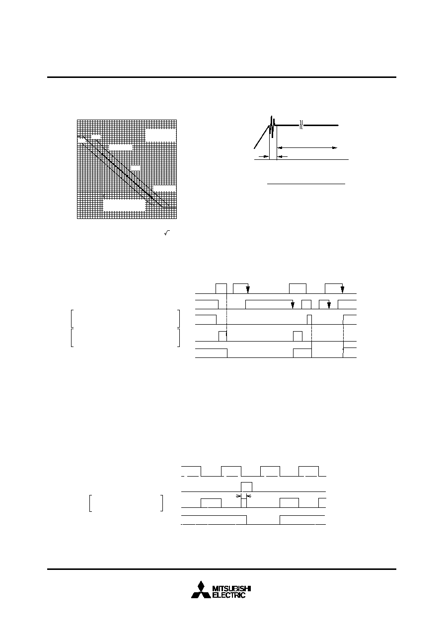
S
C
delay time
Short circuit sensing signal V
S
Error output F
O1
Gate signal Vo of each phase
upper arm(ASIPM internal)
Input signal V
CIN
of each phase
upper arm
0V
0V
0V
0V
0V
0V
0V
0V
0V
Input signal V
CIN(p)
of each phase upper arm
Input signal V
CIN(n)
of each phase lower arm
Gate signal V
o(p)
of each phase upper arm
(ASIPM internal)
Gate signal V
o(n)
of each phase upper arm
(ASIPM internal)
Error output F
O1
V
CH
(5
µ
s)
V
CH
(505
µ
s)
0V
V
C
500
µ
s
r
CH
=
V
CH
(505
µ
s)-V
CH
(5
µ
s)
V
CH
(5
µ
s)
Note ; Ringing happens around the point where the signal output
voltage changes state from "analogue" to "data hold" due
to test circuit arrangement and instrumentational trouble.
Therefore, the rate of change is measured at a 5
µ
s delayed point.
200
≠200
Analogue output signal
data hold range
1
2
3
4
5
400
300
100
0
≠100
≠300
≠400
0
V
C
+(200%)
V
C0
V
C
≠
(200%)
V
C
(V)
V
C
+
V
C
≠
min
max
Real load current peak value.(%)(I
c
=I
o
!
2)
V
DH
=15V
T
C
=
≠
20
~
100∞C
(Fig. 4)
Fig. 4 OUTPUT CURRENT ANALOGUE SIGNALING
LINEARITY
Fig. 5 OUTPUT CURRENT ANALOGUE SIGNALING
"DATA HOLD" DEFINITION
Fig. 6 INPUT INTERLOCK OPERATION TIMING CHART
Note : Input interlock protection circuit ; It is operated when the input signals for any upper-arm / lower-arm pair of a phase are simulta-
neously in "LOW" level.
By this interlocking, both upper and lower IGBTs of this mal-triggered phase are cut off, and "F
O
" signal is outputted. After an "input
interlock" operation the circuit is latched. The "F
O
" is reset by the high-to-low going edge of either an upper-leg, or a lower-leg input,
whichever comes in later.
Fig. 7 TIMING CHART AND SHORT CIRCUIT PROTECTION OPERATION
Note : Short circuit protection operation. The protection operates with "F
O
" flag and reset on a pulse-by-pulse scheme. The protection by
gate shutdown is given only to the IGBT that senses an overload (excluding the IGBT for the "Brake").