QJD0240002
Powerex, Inc., 200 Hillis St., Youngwood 15697 (724) 925-7272
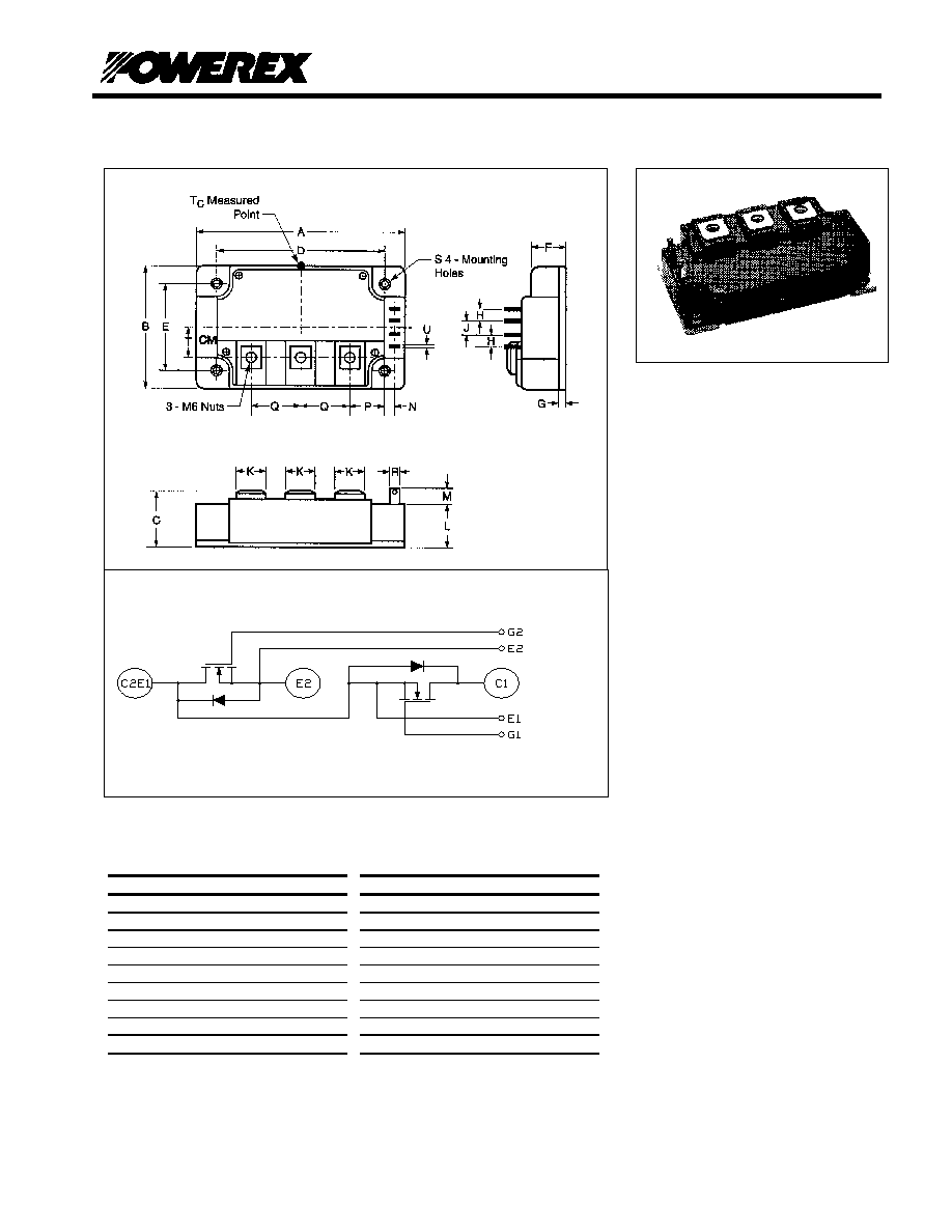
Dual Power MOSFET Module
400 Amperes/200 Volts
Preliminary Page
1 7/10/2002
Description:
Powerex Dual MOSFET Module is
designed specially for customer
applications. The module is isolated
for easy mounting with other
components on a common heatsink
.
Features:
Typical R
DS
(on) = 0.0055
Extremely High dv/td Capability
Fast Body-Drain Diode
Isolated Baseplate for Easy
Heat
Sinking
Low Thermal Impedance
Isolated Material: DBC Alumina
(4) STY100NS20FD Chips per
MOSFET Switch
Applications:
High Current, High Speed
Switching
Motor Drive
DC-AC Converter for Welding
Equipment
Switch Mode Power Supply
Dim Inches
Millimeters
A 4.25 108.0
B 2.44
62.0
C 1.14+0.04/-0.02 29+1.0/-0.5
D
3.66
±
0.01 93.0
±
0.25
E
1.88
±
0.01 48.0
±
0.25
F 0.67
17.0
G 0.16
4.0
H 0.24
6.0
J 0.59
15.0
Dim Inches
Millimeters
K 0.55
14.0
L 0.87
22.0
M 0.33
8.5
N 0.10
2.5
P 0.85
21.5
Q 0.98
25.0
R 0.11
2.8
S 0.25
Dia. 6.5
Dia.
T 0.6 15.15

QJD0240002
Powerex, Inc., 200 Hillis St., Youngwood 15697 (724) 925-7272
Dual Power MOSFET Module
400 Amperes/200 Volts
Preliminary Page
2 7/10/2002
Maximum Ratings, Tj=25
∞
∞
∞
∞
C unless otherwise specified
Ratings Symbol
QJD0240002
Units
Drain-source voltage, V
GS
=0V
V
DSS
200 Volts
Gate-source voltage
V
GSS
±
20
Volts
Drain Current at Tc = 25
∞
C
I
D
400
Amperes
Drain Current at Tc = 100
∞
C
I
D
252
Amperes
Max Operating Junction Temperature
T
j
150
∞
C
Storage Temperature
T
stg
-40 to 125
∞
C
Mounting Torque, M6 Terminal Screws
-
40
In-lb
Mounting Torque, M6 Mounting Screws
-
40
In-lb
Module Weight (Typical)
-
400
Grams
V Isolation
V
RMS
2000 Volts
Static Electrical Characteristics, Tj=25
∞
∞
∞
∞
C unless otherwise specified
Characteristic Symbol
Test
Conditions
Min.
Typ.
Max.
Units
Drain-source breakdown voltage
V
(BR)DSS
I
D
=1mA, V
GS
=0V 200 -
-
Volts
Drain leakage current
I
DSS
V
DS
=200V, V
GS
=0V -
- 40
µ
A
Drain leakage current at Tc = 125
∞
C
I
DSS
V
DS
=200V, V
GS
=0V -
- 400
µ
A
Gate leakage current
I
GSS
V
GS
=
±
20V,V
DS
=0V
- -
±
400
nA
Gate-source threshold voltage
V
GS(th)
I
D
=1mA, V
DS
=10V 3.0 4.0 5.0 Volts
Drain-source on state resistance
R
DS(ON)
I
D
=200A, V
GS
=10V - 5.5 6.0 m
Drain-source on-state voltage
V
DS (ON)
I
D
=200A, V
GS
=10V - 1.1 1.2 Volts
Forward On Voltage MOS Diode
V
SD
I
SD
=400A, V
GS
=0V -
- 1.6 Volts
Dynamic Electrical Characteristics, Tj=25
∞
∞
∞
∞
C unless otherwise specified
Characteristic Symbol
Test
Conditions
Min.
Typ.
Max.
Units
Input Capacitance
C
iss
-
31600
-
pF
Output Capacitance
C
oss
-
6000
-
pF
Reverse Transfer Capacitance
C
rss
V
DS
=25V
V
GS
=0V
f=1MHz
- 1840 -
pF
Turn on Delay time
t
d(on)
-
TBD
-
ns
Rise Time
t
r
-
TBD
-
ns
Turn- off Delay Time
t
d(off)
-
TBD
-
ns
Fall Time
t
f
V
DD
=100V
I
D
=200A
V
GS
=10V
R
G
=4.7
- TBD -
ns
Reverse Recovery Time MOS Diode
t
rr
-
225
-
ns
Reverse Recovery Charge MOS Diode
Q
rr
-
5.4
-
µC
Reverse Recovery Current MOS Diode
I
RRM
I
SD
=400A
di/dt=400A/µs
V
DD
=160V
Tj=150
∞
C
- 48 - Amperes
Thermal Characteristics, Tj=25
∞
∞
∞
∞
C unless otherwise specified
Characteristic Symbol
Test
Conditions
Min.
Typ.
Max.
Units
Thermal Resistance, Channel to Case
R
(ch-c)
Per Mosfet
-
0.08
TBD
∞
C/W
Contact Thermal Resistance
(Thermal Grease Applied)
R
CF
Per Module
-
0.020
-
∞
C/W