
Design Idea DI-35
TOPSwitch-GX
16 W Audio Amplifier Power Supply
DI-35
Æ
Application
Audio Amplifier
TOP245P
16 V
Power Output
16 W (35 W Peak)
Input Voltage
Output Voltage
Topology
Device
85-265 VAC
Flyback
Figure 1. Audio Amplifier Power Supply.
Design Highlights
∑ No heatsinks required!
∑ 77% efficiency (min), @ 85 VAC input/35 W output
∑ Low no-load input power: < 0.7 W @ 230 VAC input
∑ Low component count: 37, excluding I/O connectors
∑ Stable operation with or without 10,000
µF output buffer
capacitor
∑ Robust transformer design enables 35 W peak power
∑ Meets CISPR22B EMI with > 10 dB of margin
∑ Ideal for both class AB and class D audio amplifiers
Operation
Many of the built-in TOPSwitch-GX features have been used to
reduce the component count, transformer size, and overall cost
of this universal input flyback power supply. Designed around
a TOP245P (DIP-8 package), the device uses PCB copper for
its heatsink, eliminating the costs of both a heatsink and the
installation labor. Output diode D7 is also cooled the same way.
Resistors R1 and R2 set the nominal Under-Voltage (UV)
lockout and Overvoltage (OV) shutdown limits to 84 V and
378 V, respectively. UV lockout protects the supply from
overheating at low line and eliminates power-up and power-
down glitches. OV shutdown protects the power supply from
line surges.
The EMI filter has been significantly simplified to three
components (L1, CX1 and CY1), thanks to the built-in
frequency jitter function of the TOPSwitch-GX family.
The RCD network of C4, R3, R4, and D5 limits (clamps) the
peak voltage that the U1-DRAIN sees. A glass-passivated
normal recovery diode (D5) recycles stored leakage energy,
increasing overall efficiency. DRAIN ringing is dampened
by R4 (which is necessary when a normal recovery diode is
used).
The bias winding provides operating power and feedback
current to the CONTROL pin of U1. The U2-LED, R8 and
VR1 comprise the feedback circuit that senses the output
voltage. The current through the U2-LED regulates the
output voltage, by modulating the feedback current that
flows into the CONTROL pin of U1.
Key Design Points
∑ Ensure that the control loop has enough phase margin
at the extremes of the rated input voltage and output
load, both with and without the output buffer capacitor.
∑ A 5% VR1 should be acceptable for an audio amplifier.
Greater accuracy will require a 2% VR1.
∑ OV and UV thresholds are determined by: V
OV
=
225
µA
x
(R1+R2) and V
UV
= 50
µA
x
(R1+R2).
PI-3731-012604
16 V, 1 A / 2.2 A
RTN
U1
TOP245P
U2
U2
VR1
IN5244B
5%
CX1
220 nF
250 VAC
F1
3.15 A
250 V
85-265
VAC
N
L
C1
100
µ
F
400 V
C2
100 nF
50 V
C3
100
µ
F
16 V
U2
PC817A
D1 & D2
1N4007
D3 & D4
1N4007
CY1
2.2 nF
(Safety)
L1
6.8 mH
0.8 A
9, 10
1
3
6, 7
4
T1
5
R1
1 M
R3
200 k
1/2 W
R5
3.3
C4
1 nF
1 KV
R4
33
1/4 W
D5
IN4007G
R2
1 M
R7
10
C5
1
µ
F
50 V
D6
BAV20
R10
1 k
R8
150
R6
33
1/4 W
C6
470 pF
100 V
L2
3.3 uH
C9
100
µ
F
25 V
D7
SB5100
C10
47
µ
F
25 V
C7
470
µ
F
25 V
C8
470
µ
F
25 V
TOPSwitch-GX
D
S
C
CONTROL
M
www.powerint.com
March 2004
www.powerint.com
A
3/04
Power Integrations 5245 Hellyer Avenue
San Jose, California 95138
MAIN PHONE NUMBER
APPLICATIONS HOTLINE
APPLICATIONS FAX
For a complete listing of worldwide sales offices,
+1 408-414-9200
+1 408-414-9660
+1 408-414-9760
please visit
www.powerint.com
DI-35
The PI logo, TOPSwitch, TinySwitch, LinkSwitch and EcoSmart are registered trademarks of Power Integrations. PI Expert and DPA-Switch
are trademarks of Power Integrations. Copyright 2004, Power Integrations
Power Integrations may make changes to its products at any time. Power Integrations has no liability arising from your use of any information, device or circuit described
herein nor does it convey any license under its patent rights or the rights of others. POWER INTEGRATIONS MAKES NO WARRANTIES HEREIN AND SPECIFICALLY
DISCLAIMS ALL WARRANTIES INCLUDING, WITHOUT LIMITATION, THE IMPLIED WARRANTIES OF MERCHANTABILITY, FITNESS FOR A PARTICULAR PURPOSE,
AND NON-INFRINGEMENT OF THIRD PARTY RIGHTS. The products and applications illustrated herein (including circuits external to the products and transformer
construction) may be covered by one or more U.S. and foreign patents or potentially by pending U.S. and foreign patent applications assigned to Power Integrations.
A complete list of Power Integrations' patents may be found at www.powerint.com.
For the latest updates, visit www.powerint.com
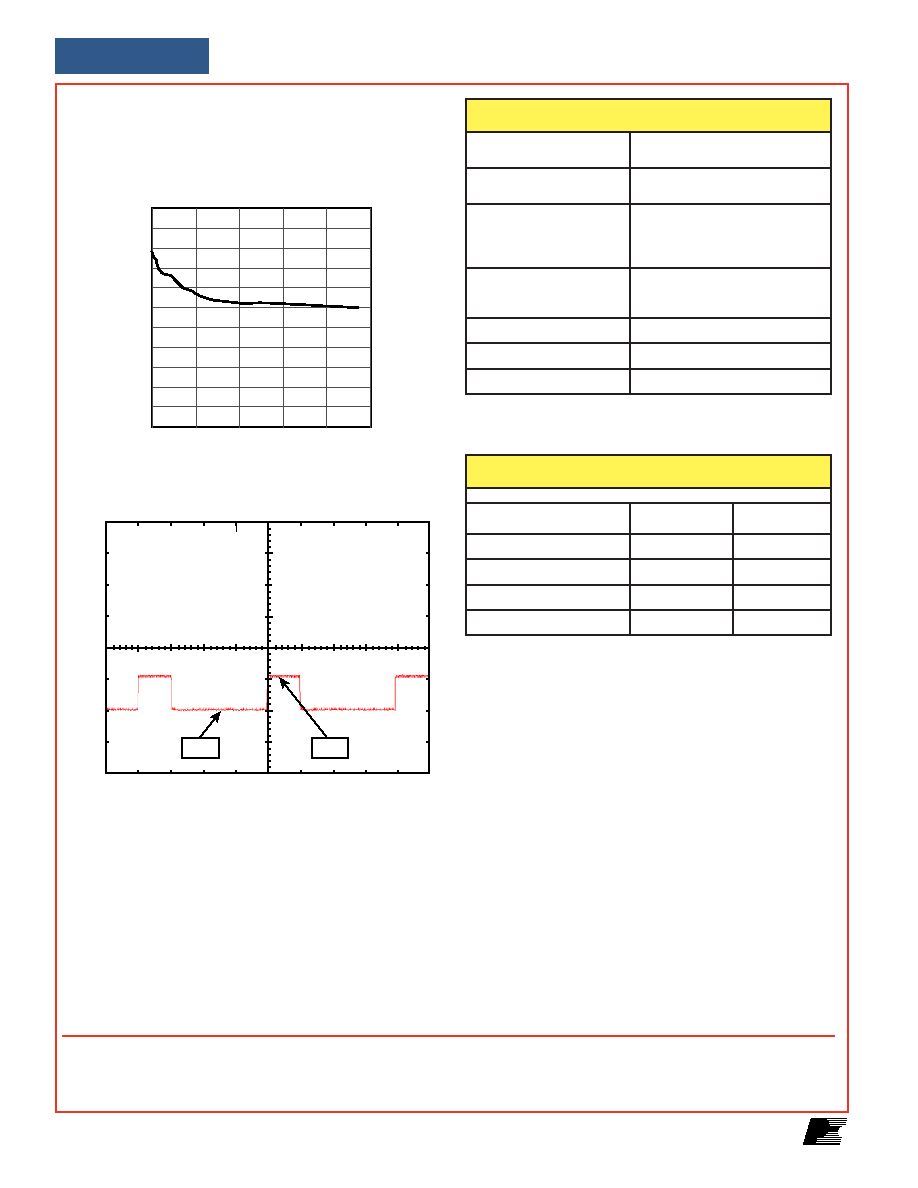
Table 1. Transformer Construction Information.
Figure 2. 115 VAC V-I Curve.
Figure 3. Load Current for Thermal Test. (10 ms/div)
TRANSFORMER PARAMETERS
Nippon Ceramic EF-25-NC-2H
A
LG
of 247 nH/T
2
Miles-Platts FE0100 with TBS-601
terminals
Primary: 65T, 2 layers, 28 AWG
Secondary: 9T, 2 x 26 AWG, Triple
Insulated
Bias: 8T, 2 x 28 AWG
Primary: 3-1, tape
Secondary: 9,10-6,7, tape,
Bias: 4-5, tape 3L
1059
µ
H
±
10%
0.75 MHz (Min)
28
µ
H (Max)
Core
Bobbin
Winding Details
Winding Order (pin numbers)
Primary Inductance
Primary Resonant Frequency
Leakage Inductance
THERMAL TEST RESULSTS
Test Case
T1 (Transformer)
U1 (TOP245P
D7 (Op Rectifier)
C8 (Op Capacitor)
T (
∞
C) @
T (
∞
C) @
85 VAC
265 VAC
57
59
64
51
58
59
41
40
Thermal test load current is 1 A for 30 ms, 2.2 A for 10 ms
Table 2. Thermal Test with Pulsed Load of Figure 3. 25
∞C
Ambiant, Open Frame, 85 VAC and 265 VAC input.
0
1
1.5
0.5
2
2.5
I
OUT
(A)
V
OUT
(V)
15.5
15.6
15.1
15.2
15.3
15.4
15
15.9
16
15.7
15.8
16.1
PI-3719-093003
PI-3730-012604
0
50
100
1
4
3
5
2
Time (ms)
Current (A)
6
7
0
-1
2.2 A
1 A
∑ Keep power loop layouts (primary and secondary) tight to
minimize noise (EMI and output ripple) and power loss.
∑ At least 10 cm
2
of PCB copper area should be used for
heatsinking.