www.powerint.com
Design Idea DI-3
TOPSwitch
Burst Mode Flyback
Design Highlights
∑ Low cost isolated converter (competitive with capacitive
dropper)
∑ DC/DC or AC/DC markets
∑ Wide range AC input applications
∑ No inductive components required in EMI filter
∑ Extremely low average EMI
∑ Surge protection without MOV
∑ Small physical size (1.2 in/30.5 mm
◊ 2.2 in/55.8 mm)
Operation
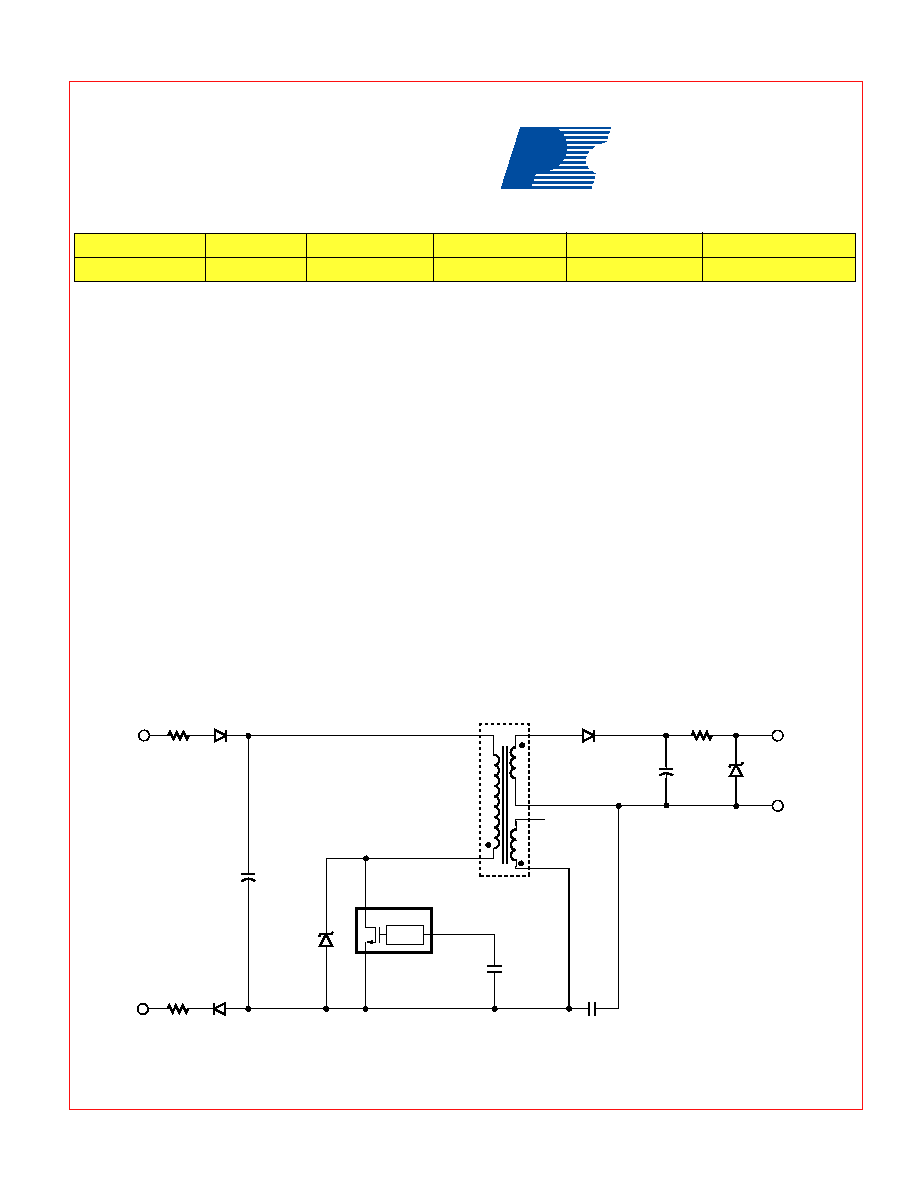
The TOPSwitch burst mode flyback supply generates a single
isolated output voltage from an AC or DC input. It is optimized
for use with the TOP221 for outputs of 0-100 mW. The basic
design can be scaled up to a maximum power of 200 mW with
a different transformer design. Typical applications are industrial
bias supplies, utility meters, and other applications requiring
extremely low system cost and low output power. The
circuit is designed to replace conventional linear supplies
and capacitor droppers, offering universal input range and
higher output power than a conventional capacitor dropper
supply.
The example shown below delivers 5.1 V at 20 mA. Input
voltage range is 85-265 VAC. Incoming AC is half-wave
rectified and averaged by R1, R2, D1, D2, and C1, providing
a DC voltage to one end of the primary winding of T1. The
other end of the transformer primary is driven by the
integrated high voltage MOSFET inside the TOP221.
C2 is charged by the TOPSwitch internal current source to
initiate operation and provide enough charge to sustain the
TOPSwitch for 8-9 switching cycles per autorestart period.
VR1 clamps the primary leakage spike at the TOPSwitch
June 1998
DI-3
Figure 1. TOPSwitch Burst Mode Flyback.
Application
Industrial Bias
TOP221P
5.1 V
Power Output
100 mW
Input Voltage
Output Voltage
Topology
Device
85 - 265 VAC
Burst Mode Flyback
Æ
POWER
INTEGRATIONS
,
INC
.
Æ
PI-2259-080398
5.1 V
RTN
C1
10
µF
400 V
C2
100 nF
D4
1N4933
C4
100
µF
35 V
T1
VR2
1N4733
R3
82
+
-
2
1
3
4
5
8
AC
INPUT
T1
D
S
C
CONTROL
TOPSwitch-II
TOP221P
U1
NC
D1
1N4007
R1
750
D2
1N4007
R2
750
Flame proof
Flame proof
VR1
P4KE550
C3
330 pF
Y1
82T
36AWG
5T
30AWG
10T
30AWG

www.powerint.com
A
6/98
DI-3
DRAIN to a safe level. The power secondary winding of T1
is rectified and filtered by D4 and C4 to provide 7.5-8 V. R3
and VR2 step down this voltage to provide a regulated 5.1 V
output. R3 is sized to provide 20 mA of output load current
and 10 mA of bias current for Zener VR2 in order to maintain
output regulation. A shunt regulator is used in this circuit to
provide a constant load to the converter since the TOPSwitch
runs open loop.
R1, R2, C1 and C3 provide EMI filtering for the power
supply. R1, R2 and C1 also protect the rest of the circuit
against input line transients. The T1 bias winding (Pins 3
and 4) does not provide power for TOPSwitch, but acts as a
shield to reduce EMI.
In this circuit, the TOP221 runs repetitively in autorestart.
The amount of power delivered in this mode is determined
by the TOPSwitch auto restart duty cycle, which sets the ratio
of switching time to idle time during autorestart, as well as the
transformer primary inductance and the TOPSwitch current
limit. With a 0.1
µF CONTROL pin capacitor, the TOP221
delivers a single burst of 8-9 pulses at 100 kHz, during each
autorestart period, with approximately 1.2 ms between
bursts.
To stabilize output power over extremes of line voltage, T1
is designed for discontinuous mode, with each switching
pulse terminated by the TOPSwitch current limit. Transformer
parameters are shown in following table.
TDK PC40EI12.5-Z or equiv.
Gap for A
L
of 208 nH/T
2
TDK BE-12.5-1110CP or equiv.
Primary (2-1), Tape, Bias (3-
4), Tape, Secondary (8-5)
1.4 mH
±
10% @ 100 kHz
700 kHz minimum
70
µ
H maximum
Core Material
Bobbin
Winding Order
Primary Inductance
(Pins 1-2, all others open)
Primary Resonant
Frequency
(Pins 1-2, all others open)
Leakage Inductance
(Pins 1-2, with Pins 5-8
shorted)
Transformer Parameters
Key Design Points
∑ Design transformer for discontinuous mode operation, with
TOPSwitch reaching current limit each cycle.
∑ Size R1, R2, and C1 to provide at least 70 VDC bus voltage
at minimum AC line voltage and maximum load.
∑ VR1 can be sourced by General Semiconductor (P4KE550).
It can be replaced by a fast recovery diode (600V PIV) and
series Zener clamp (BZY97-C200 or P6KE200) from DRAIN
to Pin 1 of the transformer, as in conventional TOPSwitch
designs.
For the latest updates, visit our Web site: www.powerint.com
Power Integrations reserves the right to make changes to its products at any time to improve reliability or manufacturability. Power
Integrations does not assume any liability arising from the use of any device or circuit described herein, nor does it convey any license
under its patent rights or the rights of others.
The PI Logo, TOPSwitch, TinySwitch and EcoSmart are registered trademarks of Power Integrations, Inc.
©Copyright 2001, Power Integrations, Inc.
KOREA
Power Integrations
International Holdings, Inc.
Seoul, Korea
Phone:
+82-2-568-7520
Fax:
+82-2-568-7474
e-mail: koreasales@powerint.com
WORLD HEADQUARTERS
AMERICAS
Power Integrations, Inc.
San Jose, CA 95138 USA
Customer Service:
Phone:
+1 408-414-9665
Fax:
+1 408-414-9765
e-mail: usasales@powerint.com
JAPAN
Power Integrations, K.K.
Keihin-Tatemono 1st Bldg.
Japan
Phone:
+81-45-471-1021
Fax:
+81-45-471-3717
e-mail: japansales@powerint.com
TAIWAN
Power Integrations
International Holdings, Inc.
Taipei, Taiwan
Phone:
+886-2-2727-1221
Fax:
+886-2-2727-1223
e-mail: taiwansales@powerint.com
EUROPE & AFRICA
Power Integrations (Europe) Ltd.
United Kingdom
Phone:
+44-1344-462-300
Fax:
+44-1344-311-732
e-mail: eurosales@powerint.com
CHINA
Power Integrations
International Holdings, Inc.
China
Phone:
+86-755-367-5143
Fax:
+86-755-377-9610
e-mail: chinasales@powerint.com
INDIA (Technical Support)
Innovatech
Bangalore, India
Phone:
+91-80-226-6023
Fax:
+91-80-228-9727
e-mail: indiasales@powerint.com
APPLICATIONS HOTLINE
World Wide +1-408-414-9660
APPLICATIONS FAX
World Wide +1-408-414-9760