
Figure 1. Typical Forward Converter Application.
Table 1. Notes: 1. Maximum output power is limited by device internal
current limit. 2. See Applications Considerations section for complete
description of assumptions and for output powers with other input voltage
ranges. 3. For device dissipation of 1.5 W or below, use P or G packages.
Device dissipation above 1.5 W is possible only with R package. 4. See
Part Ordering Information. 5. Due to higher switching losses, the DPA425
may not deliver additional power compared to a smaller device.
DPA423-426
DPA-Switch
Family
Highly Integrated DC-DC Converter ICs
for Distributed Power Architectures
The following transparent or built-in features are also provided:
soft-start, cycle skipping down to zero load and hysteretic
thermal shutdown. In addition, all critical parameters (i.e.
current limit, frequency, PWM gain) have tight temperature
and absolute tolerance, to simplify design and optimize system
cost.
Product Highlights
Highly Integrated Solution
� Eliminates 20-50 external components�saves space, cost
� Integrates 220 V high frequency MOSFET, PWM control
� Lower cost plastic DIP surface mount (G package) and
through-hole (P package) options for designs
35 W
Superior Performance and Flexibility
� Eliminates all external current sensing circuitry
� Built-in auto-restart for output overload/open loop protection
� Pin selectable 300/400 kHz fixed frequency
� Wide input (line) voltage range: 16-75 VDC
� Source connected tab reduces EMI
� Line under-voltage (UV) detection: meets ETSI standards
� Line overvoltage (OV) shutdown protection
� Low cost synchronous rectification: line UV/OV shut down
limits gate drive voltage range from transformer winding
� Fully integrated soft-start for minimum stress/overshoot
� Externally programmable current limit
� Supports forward or flyback topology
� Cycle skipping: regulation to zero load without pre-load
� Hysteretic thermal shutdown for automatic fault recovery
EcoSmart
- Energy Efficient
� Extremely low consumption at no load
� Cycle skipping at light load for high standby efficiency
Applications
� Telco central office equipment: xDSL, ISDN, PABX, etc.
� Distributed power architectures (24 V/48 V bus, etc.)
� Digital feature phones, VoIP phones, PoE
� Industrial controls (24 V/48 V)
Description
The DPA-Switch IC family introduces a highly integrated
solution for DC-DC conversion applications in the 16-75 VDC
input range.
DPA-Switch uses the same proven topology as TOPSwitch, cost
effectively integrating the high voltage power MOSFET, PWM
control, fault protection and other control circuitry onto a single
CMOS chip. High performance features are enabled with three
user configurable pins.
�
January 2004
PRODUCT
4
OUTPUT POWER TABLE
12 W 16 W
-
-
-
18 W
16 W 23 W 35 W
-
-
35 W
23 W 32 W 50 W 62 W
-
70 W
25 W 35 W 55 W 70 W 83 W 100 W
DPA423
DPA424
DPA425
DPA426
36-75 VDC INPUT RANGE (FORWARD)
2,4
Total Device
Dissipation
3
0.5 W
1 W
2.5 W
4 W
6 W
Max
Power
Output
1
PI-2770-032002
D
S
C
DPA-Switch
VIN
VO
F
X
L
CONTROL
SENSE
CIRCUIT
RESET/
CLAMP
CIRCUIT
TM
PRODUCT
4
9 W
13 W
-
-
13 W
10 W 14.5 W 18 W
24 W
26 W
-
5
-
5
-
5
25.5 W
52 W
DPA423
DPA424
DPA425
36-75 VDC INPUT RANGE (FLYBACK)
2
Total Device
3
Dissipation
0.5 W
0.75 W
1 W
1.5 W
Max
Power
Output
1

DPA423-426
2
K
1/04
Section List
Functional Block Diagram ......................................................................................................................................... 3
Pin Functional Description ........................................................................................................................................ 3
DPA-Switch Family Functional Description .............................................................................................................. 4
CONTROL (C) Pin Operation ................................................................................................................................. 4
Oscillator and Switching Frequency ....................................................................................................................... 5
Pulse Width Modulator & Maximum Duty Cycle ..................................................................................................... 6
Minimum Duty Cycle and Cycle Skipping ............................................................................................................... 6
Error Amplifier ......................................................................................................................................................... 6
On-chip Current Limit with External Programmability ............................................................................................. 6
Line Under-Voltage Detection (UV) ........................................................................................................................ 6
Line Overvoltage Shutdown (OV) ........................................................................................................................... 7
Line Feed Forward with DC
MAX
Reduction .............................................................................................................. 7
Remote ON/OFF .................................................................................................................................................... 7
Synchronization ...................................................................................................................................................... 8
Soft-Start ................................................................................................................................................................ 8
Shutdown/Auto-Restart .......................................................................................................................................... 8
Hysteretic Over-Temperature Protection ................................................................................................................ 8
Bandgap Reference ................................................................................................................................................ 8
High-Voltage Bias Current Source .......................................................................................................................... 8
Using Feature Pins ...................................................................................................................................................... 9
FREQUENCY (F) Pin Operation ............................................................................................................................. 9
LINE-SENSE (L) Pin Operation .............................................................................................................................. 9
EXTERNAL CURRENT LIMIT (X) Pin Operation ................................................................................................... 9
Typical Uses of FREQUENCY (F) Pin ...................................................................................................................... 12
Typical Uses of LINE-SENSE (L) and EXTERNAL CURRENT LIMIT (X) Pins ....................................................... 12
Application Examples ............................................................................................................................................... 15
Key Application Considerations .............................................................................................................................. 17
DPA-Switch Design Considerations ...................................................................................................................... 17
DPA-Switch Layout Considerations ...................................................................................................................... 18
Quick Design Checklist ......................................................................................................................................... 19
Design Tools ......................................................................................................................................................... 19
Product Specifications and Test Conditions .......................................................................................................... 21
Typical Performance Characteristics ..................................................................................................................... 27
Part Ordering Information ........................................................................................................................................ 31
Package Outlines ...................................................................................................................................................... 32
DPA423-426
3
K
1/04
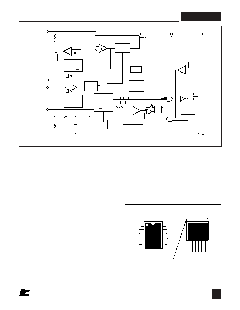
Figure 2. Functional Block Diagram.
PI-2760-070501
PI-2760-070501
SHUTDOWN/
AUTO-RESTART
PWM
COMPARATOR
CLOCK
SAW
300/400 kHz
CONTROLLED
TURN-ON
GATE DRIVER
CURRENT LIMIT
COMPARATOR
INTERNAL UV
COMPARATOR
INTERNAL
SUPPLY
5.8 V
4.8 V
SOURCE (S)
S
R
Q
DMAX
STOP SOFT-
START
-
+
CONTROL (C)
LINE-SENSE (L)
EXTERNAL
CURRENT LIMIT (X)
FREQUENCY (F)
-
+
5.8 V
1 V
IFB
RE
ZC
VC
+
-
LEADING
EDGE
BLANKING
�
8
1
HYSTERETIC
THERMAL
SHUTDOWN
SHUNT REGULATOR/
ERROR AMPLIFIER
+
-
DRAIN (D)
ON/OFF
SOFT
START
DCMAX
VBG
DCMAX
VBG + VT
0
OV/UV
VI (LIMIT)
CURRENT
LIMIT
ADJUST
LINE
SENSE
SOFT START
CYCLE
SKIPPING
STOP LOGIC
OSCILLATOR
Figure 3. Pin Configuration (top view).
Pin Functional Description
DRAIN (D) Pin:
High voltage power MOSFET drain output. The internal startup
bias current is drawn from this pin through a switched high-
voltage current source. Internal current limit sense point for
drain current.
CONTROL (C) Pin:
Error amplifier and feedback current input pin for duty cycle
control. Internal shunt regulator connection to provide internal
bias current during normal operation. It is also used as the
connection point for the supply bypass and auto-restart/
compensation capacitor.
LINE-SENSE (L) Pin:
Input pin for overvoltage (OV), under-voltage (UV) lock out,
line feed forward with the maximum duty cycle (DC
MAX
)
reduction, remote ON/OFF and synchronization. A connection
to SOURCE pin disables all functions on this pin.
EXTERNAL CURRENT LIMIT (X) Pin:
Input pin for external current limit adjustment and remote
ON/OFF. A connection to SOURCE pin disables all functions
on this pin.
PI-3822-012104
Tab Internally Connected to
SOURCE Pin (See layout considerations)
R Package
(TO-263-7C)
1 2 3 4 5
7
C L X S F
D
F
S
L
X
S
D
S
8
6
5
C
4
2
3
1
P Package (DIP-8)
G Package (SMD-8)
7
FREQUENCY (F) Pin:
Input pin for selecting switching frequency: 400 kHz if connected
to SOURCE pin and 300 kHz if connected to CONTROL pin.
SOURCE (S) Pin:
Output MOSFET source connection for the power return.
Primary side control circuit common and reference point.
DPA423-426
4
K
1/04
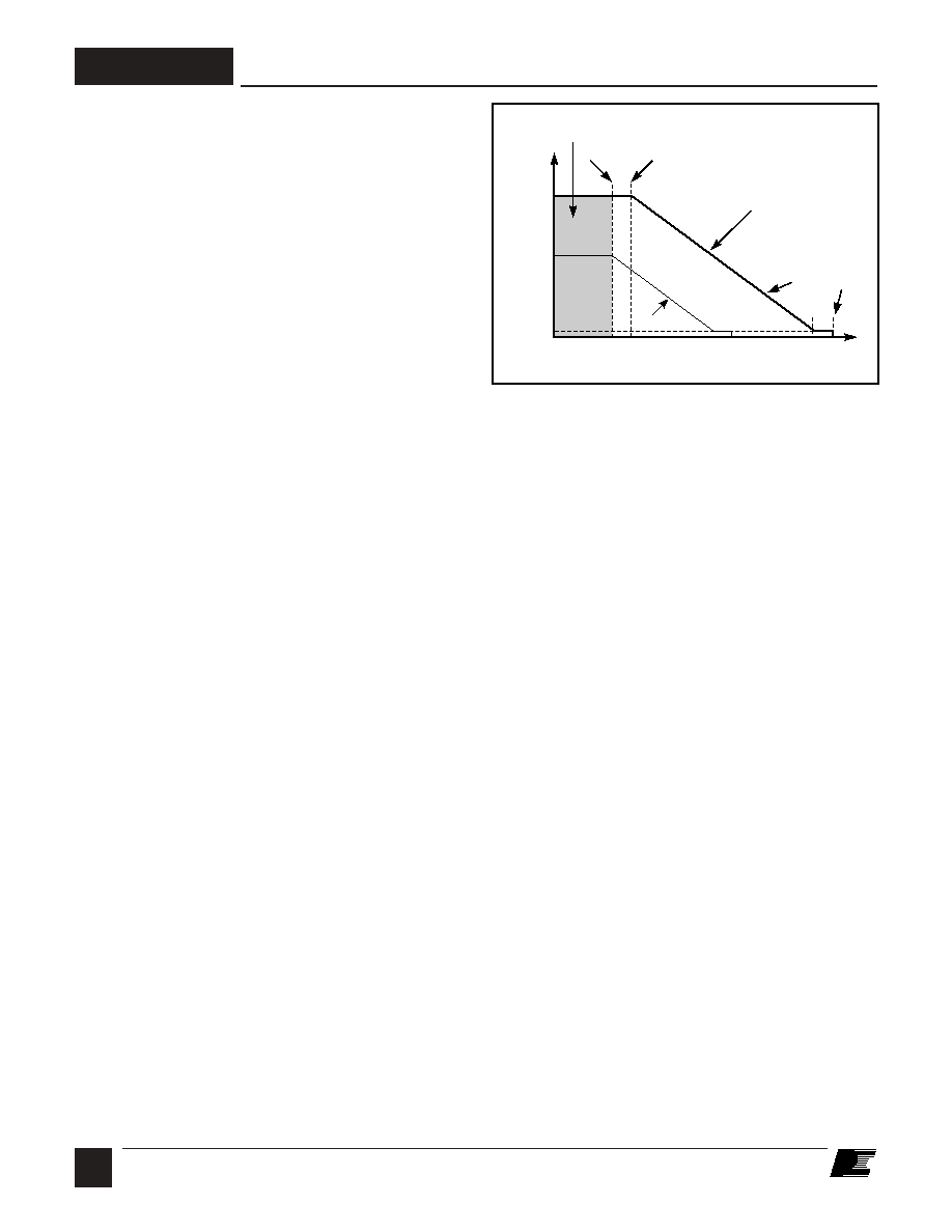
Figure 4. Relationship of Duty Cycle to CONTROL Pin Current.
DPA-Switch
Family Functional
Description
DPA-Switch is an integrated switched mode power supply chip
that converts a current at the control input to a duty cycle at the
open drain output of a high voltage power MOSFET. During
normal operation the duty cycle of the power MOSFET decreases
linearly with increasing CONTROL pin current as shown in
Figure 4. A patented high-voltage CMOS technology allows
both the high-voltage power MOSFET and all the low voltage
control circuitry to be cost effectively integrated onto a single
monolithic chip.
In addition to the standard TOPSwitch features, such as the
high-voltage start-up, the cycle-by-cycle current limiting, loop
compensation circuitry, auto-restart and thermal shutdown,
DPA-Switch also offers many advanced features that reduce
system cost and increase power supply performance and design
flexibility. Following is a summary of the advanced features:
1.
A fully integrated 5 ms soft-start limits peak currents and
voltages during start-up and reduces or eliminates output
overshoot in most applications.
2.
A 75% maximum duty cycle (DC
MAX
) together with the
line feed forward with DC
MAX
reduction feature makes
DPA-Switch well suited for both flyback and forward
topologies.
3.
High switching frequency (400 kHz/300 kHz, pin selectable)
allows the use of smaller size transformers and offers high
bandwidth for power supply control loop.
4.
Cycle skipping operation at light load minimizes standby
power consumption (typically <10 mA input current).
5.
Line under-voltage ensures glitch free operations at both
power-up and power-down and is tightly toleranced over
process and temperature to meet system level requirements
common in DC to DC converters (e.g. ETSI).
6.
Line overvoltage protects DPA-Switch against excessive
input voltage and line surge.
7.
External current limit adjustment allows the setting of the
current limit externally to a lower level near the operating
peak current and, if desired, further adjusts the level
gradually as line voltage rises. This makes possible an ideal
implementation of overload power limiting.
8.
Synchronization function allows the synchronization of
DPA-Switch operation to an external lower frequency.
9.
Remote ON/OFF feature permits DPA-Switch based power
supplies to be easily switched on/off using logic signals.
Maximum input current consumption is 2 mA in Remote
OFF.
10. Hysteretic over-temperature shutdown provides automatic
recovery from thermal fault.
11. Tight absolute tolerances and small temperature variations
on switching frequency, current limit, and under-voltage
lock out threshold (UV).
Three pins, LINE-SENSE (L), EXTERNAL CURRENT LIMIT
(X) and FREQUENCY (F), are used to implement all the pin
controllable features. A resistor from the LINE-SENSE pin to
DC input bus implements line UV, line OV and line feed
forward with DC
MAX
reduction. A resistor from the EXTERNAL
CURRENT LIMIT pin to the SOURCE pin sets current limit
externally. In addition, remote ON/OFF may be implemented
through either the LINE-SENSE pin or the EXTERNAL
CURRENT LIMIT pin depending on the polarity of the logic
signal available as well as other system specific considerations.
Shorting both the LINE-SENSE and the EXTERNAL
CURRENT LIMIT pins to the SOURCE pin disables line OV,
line UV, line feed forward with DC
MAX
reduction, external
current limit, remote ON/OFF and synchronization. The
FREQUENCY pin sets the switching frequency to 400 kHz if
connected to the SOURCE pin, or 300 kHz if connected to the
CONTROL pin. This pin should not be left open. Please refer
to "Using Feature Pins" section for detailed information
regarding the proper use of those pins.
CONTROL Pin Operation
The CONTROL pin is a low impedance node that is capable of
receiving a combined supply and feedback current. During
normal operation, a shunt regulator is used to separate the
feedback signal from the supply current. CONTROL pin
voltage V
C
is the supply voltage for the control circuitry
including the MOSFET gate driver. An external bypass capacitor
closely connected between the CONTROL and SOURCE pins
is required to supply the instantaneous gate drive current. The
total amount of capacitance connected to this pin also sets the
auto-restart timing as well as control loop compensation.
When the DC input voltage is applied to the DRAIN pin during
start-up, the MOSFET is initially off, and the CONTROL pin
capacitor is charged through the switched high voltage current
source connected internally between the DRAIN and
CONTROL pins. When the CONTROL pin voltage V
C
reaches
PI-2761-112102
Duty Cycle (%)
I
C
(mA)
I
L
= 115
�
A
I
L
<
I
L(DC)
I
C
(SKIP)
Slope = PWM Gain
I
CD1
I
B
Auto-restart
75
4
42
DPA423-426
5
K
1/04
approximately 5.8 V, the control circuitry is activated and the
soft-start begins. The soft-start circuit gradually increases the
duty cycle of the MOSFET from zero to the maximum value
over approximately 5 ms. The high voltage current source is
turned off at the end of the soft-start. If no external feedback/
supply current is fed into the CONTROL pin by the end of the
soft-start, the CONTROL pin will start discharging in response
to the supply current drawn by the control circuitry and the gate
current of the switching MOSFET driver. If the power supply
is designed properly, and no fault condition such as open loop
or overloaded output exists, the feedback loop will close,
providing external CONTROL pin current, before the
CONTROL pin voltage has had a chance to discharge to the
lower threshold voltage of approximately 4.8 V (internal supply
under-voltage lockout threshold). When the externally fed
current charges the CONTROL pin to the shunt regulator
voltage of 5.8 V, current in excess of the consumption of the
chip is shunted to SOURCE through resistor R
E
as shown in
Figure 2. This current flowing through R
E
controls the duty
cycle of the power MOSFET to provide closed loop regulation.
The shunt regulator has a finite low output impedance Z
C
that
sets the gain of the error amplifier when used in a primary
feedback configuration. The dynamic impedance Z
C
of the
CONTROL pin together with the external CONTROL pin
capacitance sets the dominant pole for the control loop.
When a fault condition such as an open loop or overloaded
output prevents the flow of an external current into the
CONTROL pin, the capacitor on the CONTROL pin discharges
towards 4.8 V. At 4.8 V auto-restart is activated which turns the
output MOSFET off and puts the control circuitry in a low
PI-2545-050602
S1
S2
S6
S7
S1
S2
S6
S7
S0
S1
S7
S0
S0
5.8 V
4.8 V
S7
0 V
0 V
0 V
V
LINE
V
C
V
DRAIN
V
OUT
Note: S0 through S7 are the output states of the auto-restart counter
2
1
2
3
4
0 V
~ ~
~ ~
~ ~
~ ~
S6
S7
~ ~
~ ~
~ ~
V
UV
~ ~
~ ~
~ ~
~ ~
S2
~ ~
Figure 5. Typical Waveforms for (1) Power Up (2) Normal Operation (3) Auto-restart (4) Power Down.
current standby mode. The high-voltage current source turns on
and charges the external capacitance again. A hysteretic
internal supply under-voltage comparator keeps V
C
within a
window of typically 4.8 to 5.8 V by turning the high-voltage
current source on and off as shown in Figure 5. The auto-restart
circuit has a divide-by-8 counter that prevents the output
MOSFET from turning on again until eight discharge/charge
cycles have elapsed. This is accomplished by enabling the
output MOSFET only when the divide-by-8 counter reaches
full count (S7). The counter effectively limits DPA-Switch
power dissipation as well as the maximum power delivered to
the power supply output by reducing the auto-restart duty cycle
to typically 4%. Auto-restart mode continues until output
voltage regulation is again achieved through closure of the
feedback loop.
Oscillator and Switching Frequency
The internal oscillator linearly charges and discharges an internal
capacitance between two voltage levels to create a sawtooth
waveform for the pulse width modulator. The oscillator sets
both the pulse width modulator latch and the current limit latch
at the beginning of each cycle.
The nominal switching frequency of 400 kHz was chosen to
minimize the transformer size and to allow faster power supply
loop response. The FREQUENCY pin, when shorted to the
CONTROL pin, lowers the switching frequency to 300 kHz,
which may be preferable in some applications such as those
employing secondary synchronous rectification. Otherwise,
the FREQUENCY pin should be connected to the SOURCE pin
for the default 400 kHz.