 | –≠–ª–µ–∫—Ç—Ä–æ–Ω–Ω—ã–π –∫–æ–º–ø–æ–Ω–µ–Ω—Ç: INT100 | –°–∫–∞—á–∞—Ç—å:  PDF PDF  ZIP ZIP |

June 1996
INT100
Half-Bridge Driver IC
Low-Side and High-side Drive
with Simultaneous Conduction Lockout
Product Highlights
5 V CMOS Compatible Control Inputs
∑ Combines logic inputs for low and high-side drives
∑ Schmidt-triggered inputs for noise immunity
Built-in High-voltage Level Shifters
∑ Can withstand up to 800 V for direct interface to the HV-
referenced high-side switch
∑ Pulsed internal high-voltage level shifters reduce power
consumption
Gate Drive Outputs for External MOSFETs
∑ Provides 300 mA sink/150 mA source current
∑ Can drive MOSFET gates at up to 15 V
∑ External MOSFET allows flexibility in design for various
motor sizes
Built-in Protection Features
∑ Simultaneous conduction lockout protection
∑ Undervoltage lockout
Description
The INT100 half-bridge driver IC provides gate drive for
external low-side and high-side MOSFET switches. The INT100
provides a simple, cost-effective interface between low-voltage
control logic and high-voltage loads. The INT100 is designed
to be used with rectified 110 V or 220 V supplies. Both high-
side and low-side switches can be controlled independently
from ground-referenced 5 V logic inputs.
Built-in protection logic prevents both switches from turning
on at the same time and shorting the high voltage supply. Pulsed
internal level shifting saves power and provides enhanced noise
immunity. The circuit is powered from a nominal 15 V supply
to provide adequate gate drive for external N-channel MOSFETs.
A floating high-side supply is derived from the low-voltage rail
by using a simple bootstrap technique.
Applications for the INT100 include motor drives, electronic
ballasts, and uninterruptible power supplies. Multiple devices
can also be used to implement full-bridge and multi-phase
configurations.
The INT100 is available in a 16-pin plastic SOIC package.
Æ
Figure 1. Typical Application
ORDERING INFORMATION
N/C
PI-1067-101493
VDDH
HS RTN
HS RTN
HS OUT
N/C
N/C
VDD
HS IN
LS IN
COM
LS RTN
LS OUT
16
15
14
13
12
11
10
9
1
2
3
4
5
6
7
8
HS RTN
COM
N/C
Figure 2. Pin Configuration.
HV
HS IN
LS IN
COM
LS
RTN
HS RTN
HS OUT
LS OUT
INT100
PI-1807-031296
VDD
V
DDH
PART
NUMBER
INT100S
ISOLATION
VOLTAGE
800 V
S16A
PACKAGE
OUTLINE

INT100
C
6/96
2
HS IN
LS IN
COM
PI-1083A-013194
PULSE
CIRCUIT
LINEAR
REGULATOR
VDD
DELAY
UV
LOCKOUT
VDDH
HS RTN
LS OUT
LS RTN
HS OUT
LINEAR
REGULATOR
UV
LOCKOUT
DISCRIMINATOR
DELAY
R
Q
S
Figure 3. Functional Block Diagram of the INT100

C
6/96
INT100
3
Pin Functional Description
Pin 1:
V
DD
supplies power to the logic, high-
side interface, and low-side driver.
Pin 2:
Active-low logic level input
HS IN
HS IN
HS IN
HS IN
HS IN
controls the high-side driver output.
Pin 3:
Active-high logic level input LS IN
controls the low-side driver output.
Pin 4, 5:
COM connection is used as the analog
reference point for the circuit.
Pin 7:
LS RTN is the power reference point for
the low-side circuitry, and should be
connected to the source of the low-side
MOSFET and to the COM pin.
Pin 8:
LS OUT is the driver output which
controls the low-side MOSFET.
Pin 11:
HS OUT is the driver output which
controls the high-side MOSFET.
Pin 12,13,14:
HS RTN is the power reference point
for the high-side circuitry, and should be
connected to the source of the high-side
MOSFET.
Pin 15:
V
DDH
supplies power to the high-side
control logic and output driver. This is
normally connected to a high-side
referenced bootstrap circuit or can be
supplied from a separate floating power
supply.
INT100 Functional Description
5 V Regulators
Both low-side and high-side driver
circuits incorporate a 5 V linear regulator
circuit. The low-side regulator provides
the supply voltage for the control logic
and high-voltage level shift circuit. This
allows
HS IN and LS IN to be directly
compatible with 5 V CMOS logic
without the need of an external 5 V
supply. The high-side regulator provides
the supply voltage for the noise rejection
circuitry and high-side control logic.
Undervoltage Lockout
The undervoltage lockout circuit for the
low-side driver disables both the LS
OUT and HS OUT pins whenever the
V
DD
power supply falls below typically
9.0 V, and maintains this condition until
the V
DD
power supply rises above
typically 9.35 V. This guarantees that
both MOSFETs will remain off during
power-up or fault conditions.
The undervoltage lockout circuit for the
high-side driver disables the HS OUT
pin whenever the V
DDH
power supply
falls below typically 9.0 V, and maintains
this condition until the V
DDH
power
supply rises above typically 9.35 V.
This guarantees that the high-side
MOSFET will be off during power-up
or fault conditions.
Level Shift
The level shift control circuitry of the
low-side driver is connected to integrated
high-voltage N-channel MOSFET
transistors which perform the level-
shifting function for communication to
the high-side driver. Controlled current
capability allows the drain voltage to
float with the high-side driver. Two
individual channels produce a true
differential communication channel for
accurately controlling the high-side
driver in the presence of fast moving
high-voltage waveforms. The high
voltage level shift transistors employed
exhibit very low output capacitance,
minimizing the displacement currents
between the low-side and high-side
drivers during fast moving voltage
transients created during switching of
the external MOSFETs. As a result,
power dissipation is minimized and noise
immunity optimized.
The pulse circuit provides the two high-
voltage level shifters with precise timing
signals. These signals are used by the
discriminator to reject spurious noise.
The combination of differential
communication with the precise timing
provides maximum immunity to noise.
Simultaneous Conduction Lockout
A latch prevents the low-side driver and
high-side driver from being on at the
same time, regardless of the input signals.
Delay Circuit
The delay circuit matches the low-side
propagation delay with the combination
of the pulse circuit, high voltage level
shift, and high-side driver propagation
delays. This ensures that the low-side
driver and high-side driver will never be
on at the same time during switching
transitions in either direction.
Driver
The CMOS drive circuitry on both low-
side and high-side driver ICs provide
drive power to the gates of the external
MOSFETs. The drivers consist of a
CMOS buffer capable of driving external
transistor gates at up to 15 V.
INT100
C
6/96
4
100
0
0
100
200
Gate Charge (nC)
Switching Frequncy (kHz)
200
300
400
PI-1663-112095
VIN = 200 V
VIN = 300 V
VIN = 400 V
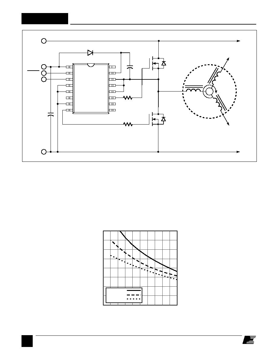
Figure 4. Using the INT100 in a 3-phase Configuration.
Figure 5. Gate Charge versus Switching Frequency.
PI-1458-042695
HV+
VDD
LS IN
HV-
INT100
PHASE 1
PHASE 2
PHASE 3
D1
C1
C2
R2
R1
Q2
Q1
HS IN
16
15
14
13
12
11
10
9
1
2
3
4
5
6
7
8

C
6/96
INT100
5
General Circuit Operation
observed. The order of signal application
should be V
DD
, logic signals, and then
HV+. V
DD
should be supplied from a
low impedance voltage source.
The output returns (HS RTN and LS
RTN) are isolated from one another by
the internal high-voltage MOSFET level
shifters. The level shift circuitry is
designed to operate properly even when
the HS RTN swings as much as 5 V
below the LS RTN pin with V
DDH
biased
at 15 V. The INT100 will also safely
tolerate more negative voltages (as low
as -V
DDH
below LS RTN).
Maximum frequency of operation is
limited by power dissipation due to high-
voltage switching, gate charge, and bias
power. Figure 5 indicates the maximum
switching frequency as a function of
input voltage and gate charge. For higher
ambient temperatures, the switching
frequency should be derated linearly.
One phase of a three-phase motor drive
circuit is shown in Figure 4 to illustrate
an application of the INT100. The LS
IN signal directly controls MOSFET
Q1. The
HS IN signal controls MOSFET
Q2 via the high voltage level shift
transistors communicating with the high-
side driver. The INT100 will ignore
input signals that would command both
Q1 and Q2 to conduct simultaneously,
protecting against shorting the HV+ bus
to HV-.
Local bypassing for the low-side driver
is provided by C1. Bootstrap bias for the
high-side driver is provided by D1 and
C2. Slew rate and effects of parasitic
oscillations in the load waveforms are
controlled by resistors R1 and R2.
The inputs are designed to be compatible
with 5 V CMOS logic levels and should
not be connected to V
DD
. Normal CMOS
power supply sequencing should be
The bootstrap capacitor must be large
enough to provide bias current over the
entire on-time of the high-side driver
without significant voltage sag or decay.
The high-side MOSFET gate charge
must also be supplied at the desired
switching frequency. Figure 6 shows
the maximum high-side on-time versus
gate charge of the external MOSFET.
Applications with extremely long high-
side on times require special techniques
discussed in AN-10.
The high-side driver is latched on and
off by the edges of the appropriate low-
side logic signal. The high-side driver
will latch off and stay off if the bootstrap
capacitor discharges below the
undervoltage lockout threshold.
Undervoltage lockout-induced turn off
can occur during conditions such as
power ramp up, motor start, or low speed
operation.
Figure 6. High-side On Time versus Bootstrap Capacitor.
1000
0.1
0.01
0.01
0.1
1
10
100
High Side On Time (ms)
Bootstrap Capacitance (
µ
F)
C
BOOTSTRAP
vs. ON TIME
1
100
PI-566B-030692
10
QG = 20 nC
QG = 100 nC